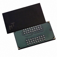
MT48H8M16LFB4-10 Micron Technology Inc, MT48H8M16LFB4-10 Datasheet - Page 38

MT48H8M16LFB4-10
Manufacturer Part Number
MT48H8M16LFB4-10
Description
IC SDRAM 128MBIT 100MHZ 54VFBGA
Manufacturer
Micron Technology Inc
Datasheet
1.MT48H8M16LFB4-8_IT_TR.pdf
(64 pages)
Specifications of MT48H8M16LFB4-10
Format - Memory
RAM
Memory Type
Mobile SDRAM
Memory Size
128M (8Mx16)
Speed
100MHz
Interface
Parallel
Voltage - Supply
1.7 V ~ 1.9 V
Operating Temperature
0°C ~ 70°C
Package / Case
54-VFBGA
Lead Free Status / RoHS Status
Lead free / RoHS Compliant
Available stocks
Company
Part Number
Manufacturer
Quantity
Price
Company:
Part Number:
MT48H8M16LFB4-10
Manufacturer:
MICRON
Quantity:
11 200
Company:
Part Number:
MT48H8M16LFB4-10
Manufacturer:
MICRON
Quantity:
7 309
Company:
Part Number:
MT48H8M16LFB4-10
Manufacturer:
Micron Technology Inc
Quantity:
10 000
PDF: 09005aef80c97087/Source: 09005aef80c97015
MT48H8M16_2.fm - Rev. E 3/05 EN
10. For a READ without auto precharge interrupted by a READ (with or without auto pre-
11. For a READ without auto precharge interrupted by a WRITE (with or without auto pre-
12. For a WRITE without auto precharge interrupted by a READ (with or without auto pre-
13. For a WRITE without auto precharge interrupted by a WRITE (with or without auto pre-
14. For a READ with auto precharge interrupted by a READ (with or without auto precharge),
15. For a READ with auto precharge interrupted by a WRITE (with or without auto precharge),
16. For a WRITE with auto precharge interrupted by a READ (with or without auto precharge),
17. For a WRITE with auto precharge interrupted by a WRITE (with or without auto pre-
7. READs or WRITEs to bank m listed in the Command (Action) column include READs or
8. CONCURRENT AUTO PRECHARGE: Bank n will initiate the auto precharge command when
9. Burst in bank n continues as initiated.
WRITEs with auto precharge enabled and READs or WRITEs with auto precharge disabled.
its burst has been interrupted by bank m’s burst.
charge), the READ to bank m will interrupt the READ on bank n, CAS latency later
(Figure 10 on page 21).
charge), the WRITE to bank m will interrupt the READ on bank n when registered
(Figure 12 and Figure 13 on page 23). DQM should be used one clock prior to the WRITE
command to prevent bus contention.
charge), the READ to bank m will interrupt the WRITE on bank n when registered
(Figure 20 on page 27), with the data-out appearing CAS latency later. The last valid
WRITE to bank n will be data-in registered one clock prior to the READ to bank m.
charge), the WRITE to bank m will interrupt the WRITE on bank n when registered
(Figure 18 on page 26). The last valid WRITE to bank n will be data-in registered one clock
prior to the READ to bank m.
the READ to bank m will interrupt the READ on bank n, CAS latency later (Figure 27 on
page 32). The PRECHARGE to bank n will begin when the READ to bank m is registered.
the WRITE to bank m will interrupt the READ on bank n when registered (Figure 28 on
page 32). DQM should be used two clocks prior to the WRITE command to prevent bus
contention. The PRECHARGE to bank n will begin when the WRITE to bank m is registered.
the READ to bank m will interrupt the WRITE on bank n when registered, with the data-
out appearing CAS latency later (Figure 29 on page 33). The PRECHARGE to bank n will
begin after
valid WRITE bank n will be data-in registered one clock prior to the READ to bank m.
charge), the WRITE to bank m will interrupt the WRITE on bank n when registered. The
PRECHARGE to bank n will begin after
bank m is registered (Figure 30 on page 33). The last valid WRITE to bank n will be data
registered one clock to the WRITE to bank m.
t
WR is met, where
38
t
WR begins when the READ to bank m is registered. The last
Micron Technology, Inc., reserves the right to change products or specifications without notice.
t
WR is met, where
128Mb: x16 Mobile SDRAM
t
WR begins when the WRITE to
©2003 Micron Technology, Inc. All rights reserved.
Power-Down


