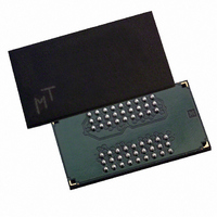
MT48H8M16LFB4-10 Micron Technology Inc, MT48H8M16LFB4-10 Datasheet - Page 18

MT48H8M16LFB4-10
Manufacturer Part Number
MT48H8M16LFB4-10
Description
IC SDRAM 128MBIT 100MHZ 54VFBGA
Manufacturer
Micron Technology Inc
Datasheet
1.MT48H8M16LFB4-8_IT_TR.pdf
(64 pages)
Specifications of MT48H8M16LFB4-10
Format - Memory
RAM
Memory Type
Mobile SDRAM
Memory Size
128M (8Mx16)
Speed
100MHz
Interface
Parallel
Voltage - Supply
1.7 V ~ 1.9 V
Operating Temperature
0°C ~ 70°C
Package / Case
54-VFBGA
Lead Free Status / RoHS Status
Lead free / RoHS Compliant
Available stocks
Company
Part Number
Manufacturer
Quantity
Price
Company:
Part Number:
MT48H8M16LFB4-10
Manufacturer:
MICRON
Quantity:
11 200
Company:
Part Number:
MT48H8M16LFB4-10
Manufacturer:
MICRON
Quantity:
7 309
Company:
Part Number:
MT48H8M16LFB4-10
Manufacturer:
Micron Technology Inc
Quantity:
10 000
Deep Power-Down
Operation
Bank/Row Activation
PDF: 09005aef80c97087/Source: 09005aef80c97015
MT48H8M16_2.fm - Rev. E 3/05 EN
The procedure for exiting self refresh requires a sequence of commands. First, CLK must
be stable (stable clock is defined as a signal cycling within timing constraints specified
for the clock pin) prior to CKE going back HIGH. Once CKE is HIGH, the SDRAM must
have NOP commands issued (a minimum of two clocks) for
required for the completion of any internal refresh in progress.
Upon exiting the self refresh mode, AUTO REFRESH commands should be issued at
once and then every 15.625µs or less, as both SELF REFRESH and AUTO REFRESH uti-
lize the row refresh counter.
The operating mode deep power-down achieves maximum power reduction by elimi-
nating the power of the whole memory array of the device. Array data will not be
retained once the device enters deep power-down mode.
This mode is entered by having all banks idle then CS# and WE# held LOW with RAS#
and CAS# held HIGH at the rising edge of the clock, while CKE is LOW. This mode is
exited by asserting CKE HIGH.
Before any READ or WRITE commands can be issued to a bank within the SDRAM, a row
in that bank must be “opened.” This is accomplished via the ACTIVE command, which
selects both the bank and the row to be activated (see Figure 7 on page 19).
After opening a row (issuing an ACTIVE command), a READ or WRITE command may be
issued to that row, subject to the
the clock period and rounded up to the next whole number to determine the earliest
clock edge after the ACTIVE command on which a READ or WRITE command can be
entered. For example, a
results in 2.5 clocks, rounded to 3. This is reflected in Figure 8 on page 19, which covers
any case where 2 <
specification limits from time units to clock cycles.)
A subsequent ACTIVE command to a different row in the same bank can only be issued
after the previous active row has been “closed” (precharged). The minimum time inter-
val between successive ACTIVE commands to the same bank is defined by
A subsequent ACTIVE command to another bank can be issued while the first bank is
being accessed, which results in a reduction of total row-access overhead. The minimum
time interval between successive ACTIVE commands to different banks is defined by
t
RRD.
t
RCD (MIN)/
t
RCD specification of 20ns with a 125 MHz clock (8ns period)
18
t
t
CK ≤ 3. (The same procedure is used to convert other
RCD specification.
Micron Technology, Inc., reserves the right to change products or specifications without notice.
t
128Mb: x16 Mobile SDRAM
RCD (MIN) should be divided by
t
XSR because time is
©2003 Micron Technology, Inc. All rights reserved.
Deep Power-Down
t
RC.


