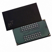
MT48H8M16LFB4-10 Micron Technology Inc, MT48H8M16LFB4-10 Datasheet - Page 11

MT48H8M16LFB4-10
Manufacturer Part Number
MT48H8M16LFB4-10
Description
IC SDRAM 128MBIT 100MHZ 54VFBGA
Manufacturer
Micron Technology Inc
Datasheet
1.MT48H8M16LFB4-8_IT_TR.pdf
(64 pages)
Specifications of MT48H8M16LFB4-10
Format - Memory
RAM
Memory Type
Mobile SDRAM
Memory Size
128M (8Mx16)
Speed
100MHz
Interface
Parallel
Voltage - Supply
1.7 V ~ 1.9 V
Operating Temperature
0°C ~ 70°C
Package / Case
54-VFBGA
Lead Free Status / RoHS Status
Lead free / RoHS Compliant
Available stocks
Company
Part Number
Manufacturer
Quantity
Price
Company:
Part Number:
MT48H8M16LFB4-10
Manufacturer:
MICRON
Quantity:
11 200
Company:
Part Number:
MT48H8M16LFB4-10
Manufacturer:
MICRON
Quantity:
7 309
Company:
Part Number:
MT48H8M16LFB4-10
Manufacturer:
Micron Technology Inc
Quantity:
10 000
Figure 4: Mode Register Definition
Burst Type
CAS Latency
PDF: 09005aef80c97087/Source: 09005aef80c97015
MT48H8M16_2.fm - Rev. E 3/05 EN
Note:
to prevent Extended
Accesses within a given burst may be programmed to be either sequential or interleaved;
this is referred to as the burst type and is selected via bit M3.
The ordering of accesses within a burst is determined by the burst length, the burst type,
and the starting column address, as shown in Table 4, "Burst Definition," on page 10.
The CAS latency is the delay, in clock cycles, between the registration of a READ com-
mand and the availability of the first piece of output data. The latency can be set to one,
two, or three clocks.
If a READ command is registered at clock edge n, and the latency is m clocks, the data
will be available by clock edge n + m. The DQs will start driving as a result of the clock
edge one cycle earlier (n + m - 1), and provided that the relevant access times are met,
** BA1, BA0 = “0, 0”
Mode Register.
The remaining (least significant) address bit(s) is (are) used to select the starting location
within the block. Full-page bursts wrap within the page if the boundary is reached.
to ensure compatibility
with future devices.
Reserved**
*Should program
13
M13
BA1
M10 = “0, 0”
12
M12
BA0
Reserved* WB
11
A11
M11
10
M10
A10
M9
0
1
9
M9
A9
Op Mode
M8
8
A8
7
M7 M6
A7 A6
Programmed Burst Length
M8
0
Single Location Access
CAS Latency
-
6
Write Burst Mode
5
M5
A5
M7
0
-
11
4
M4
A4
M3
BT
Defined
M6-M0
0
1
3
M3
A3
-
M6
M2
0
0
0
0
1
1
1
1
0
0
0
0
1
1
1
1
Burst Length
2
M2
M1
M5
A2
0
0
1
1
0
0
1
1
0
0
1
1
0
0
1
1
M0
M4
1
0
1
0
1
0
1
0
1
0
1
0
1
0
1
0
1
M1
A1
Micron Technology, Inc., reserves the right to change products or specifications without notice.
0
All other states reserved
M0
A0
Reserved
Reserved
Reserved
Full Page
Standard Operation
M3 = 0
Operating Mode
Burst Type
Interleaved
Sequential
1
2
4
8
Mode Register (Mx)
Address Bus
Burst Length
CAS Latency
Reserved
Reserved
Reserved
Reserved
Reserved
1
2
3
Reserved
Reserved
Reserved
Reserved
M3 = 1
1
2
4
8
128Mb: x16 Mobile SDRAM
Mode Register Definition
©2003 Micron Technology, Inc. All rights reserved.


