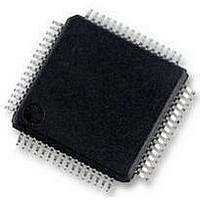
HD64F36077GHV Renesas Electronics America, HD64F36077GHV Datasheet - Page 139

HD64F36077GHV
Manufacturer Part Number
HD64F36077GHV
Description
16BIT MCU FLASH 56K, SMD, LQFP64
Manufacturer
Renesas Electronics America
Datasheet
1.HD64F36077GHV.pdf
(524 pages)
Specifications of HD64F36077GHV
No. Of I/o's
47
Ram Memory Size
4KB
Cpu Speed
20MHz
No. Of Timers
4
Digital Ic Case Style
LQFP
Supply Voltage Range
4.5V
Core Size
16bit
Program Memory Size
56KB
Oscillator Type
External Only
Controller Family/series
H8/300H
Peripherals
ADC
Rohs Compliant
Yes
Lead Free Status / RoHS Status
Lead free / RoHS Compliant
Available stocks
Company
Part Number
Manufacturer
Quantity
Price
Company:
Part Number:
HD64F36077GHV
Manufacturer:
RENESAS
Quantity:
340
Part Number:
HD64F36077GHV
Manufacturer:
RENESAS/瑞萨
Quantity:
20 000
- Current page: 139 of 524
- Download datasheet (4Mb)
7.3
There are two modes for programming/erasing of the flash memory; boot mode, which enables on-
board programming/erasing, and programmer mode, in which programming/erasing is performed
with a PROM programmer. On-board programming/erasing can also be performed in user
program mode. At reset-start in reset mode, this LSI changes to a mode depending on the TEST
pin settings, NMI pin settings, and input level of each port, as shown in table 7.1. The input level
of each pin must be defined four states before the reset ends.
When changing to boot mode, the boot program built into this LSI is initiated. The boot program
transfers the programming control program from the externally-connected host to on-chip RAM
via SCI3. After erasing the entire flash memory, the programming control program is executed.
This can be used for programming initial values in the on-board state or for a forcible return when
programming/erasing can no longer be done in user program mode. In user program mode,
individual blocks can be erased and programmed by branching to the user program/erase control
program prepared by the user.
Table 7.1
[Legend] X: Don't care.
7.3.1
Table 7.2 shows the boot mode operations between reset end and branching to the programming
control program.
1. When boot mode is used, the flash memory programming control program must be prepared in
2. SCI3 should be set to asynchronous mode, and the transfer format as follows: 8-bit data, 1 stop
3. When the boot program is initiated, the chip measures the low-level period of asynchronous
TEST
0
0
1
the host beforehand. Prepare a programming control program in accordance with the
description in section 7.4, Flash Memory Programming/Erasing.
bit, and no parity.
SCI communication data (H'00) transmitted continuously from the host. The chip then
calculates the bit rate of transmission from the host, and adjusts the SCI3 bit rate to match that
of the host. The reset should end with the RxD pin high. The RxD and TxD pins should be
On-Board Programming Modes
Boot Mode
NMI
1
0
X
Setting Programming Modes
P85
X
1
X
PB0
X
X
0
PB1
X
X
0
X
X
0
PB2
Rev. 1.00 Sep. 16, 2005 Page 109 of 490
User Mode
LSI State after Reset End
Boot Mode
Programmer Mode
REJ09B0216-0100
Section 7 ROM
Related parts for HD64F36077GHV
Image
Part Number
Description
Manufacturer
Datasheet
Request
R

Part Number:
Description:
KIT STARTER FOR M16C/29
Manufacturer:
Renesas Electronics America
Datasheet:

Part Number:
Description:
KIT STARTER FOR R8C/2D
Manufacturer:
Renesas Electronics America
Datasheet:

Part Number:
Description:
R0K33062P STARTER KIT
Manufacturer:
Renesas Electronics America
Datasheet:

Part Number:
Description:
KIT STARTER FOR R8C/23 E8A
Manufacturer:
Renesas Electronics America
Datasheet:

Part Number:
Description:
KIT STARTER FOR R8C/25
Manufacturer:
Renesas Electronics America
Datasheet:

Part Number:
Description:
KIT STARTER H8S2456 SHARPE DSPLY
Manufacturer:
Renesas Electronics America
Datasheet:

Part Number:
Description:
KIT STARTER FOR R8C38C
Manufacturer:
Renesas Electronics America
Datasheet:

Part Number:
Description:
KIT STARTER FOR R8C35C
Manufacturer:
Renesas Electronics America
Datasheet:

Part Number:
Description:
KIT STARTER FOR R8CL3AC+LCD APPS
Manufacturer:
Renesas Electronics America
Datasheet:

Part Number:
Description:
KIT STARTER FOR RX610
Manufacturer:
Renesas Electronics America
Datasheet:

Part Number:
Description:
KIT STARTER FOR R32C/118
Manufacturer:
Renesas Electronics America
Datasheet:

Part Number:
Description:
KIT DEV RSK-R8C/26-29
Manufacturer:
Renesas Electronics America
Datasheet:

Part Number:
Description:
KIT STARTER FOR SH7124
Manufacturer:
Renesas Electronics America
Datasheet:

Part Number:
Description:
KIT STARTER FOR H8SX/1622
Manufacturer:
Renesas Electronics America
Datasheet:


