DSP56309EVM Freescale Semiconductor, DSP56309EVM Datasheet - Page 86
DSP56309EVM
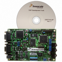
Manufacturer Part Number
DSP56309EVM
Description
KIT EVALUATION FOR XC56309
Manufacturer
Freescale Semiconductor
Type
DSPr
Specifications of DSP56309EVM
Contents
Module Board, Installation Guide, Power Supply, Cable, Software and more
Description/function
Audio DSPs
Product
Audio Modules
For Use With/related Products
DSP56309
Lead Free Status / RoHS Status
Contains lead / RoHS non-compliant


Core Configuration
4.7 DMA Control Registers 5–0 (DCR[5–0])
The DMA Control Registers (DCR[5–0]) are read/write registers that control the DMA operation
for each of their respective channels. All DCR bits are cleared during processor reset.
4-28
Number
Number
1–0
Bit
Bit
DRS0
23
22
DE
23
11
Bit Name
Bit Name
D3D
BAT
DIE
DIE
22
10
DE
Table 4-10. Address Attribute Registers (AAR[0–3]) Bit Definitions
DTM2
DAM5
Table 4-11. DMA Control Register (DCR) Bit Definitions
Reset
Reset
Value
Value
21
9
0
0
0
DTM1
DAM4
DMA Channel Enable
Enables the channel operation. Setting DE either triggers a single block DMA transfer in the
DMA transfer mode that uses DE as a trigger or enables a single-block, single-line, or
single-word DMA transfer in the transfer modes that use a requesting device as a trigger.
DE is cleared by the end of DMA transfer in some of the transfer modes defined by the DTM
bits. If software explicitly clears DE during a DMA operation, the channel operation stops
only after the current DMA transfer completes (that is, the current word is stored into the
destination).
DMA Interrupt Enable
Generates a DMA interrupt at the end of a DMA block transfer after the counter is loaded
with its preloaded value. A DMA interrupt is also generated when software explicitly clears
DE during a DMA operation. Once asserted, a DMA interrupt request can be cleared only
by the service of a DMA interrupt routine. To ensure that a new interrupt request is not
generated, clear DIE while the DMA interrupt is serviced and before a new DMA request is
generated at the end of a DMA block transfer—that is, at the beginning of the DMA channel
interrupt service routine. When DIE is cleared, the DMA interrupt is disabled.
Bus Access Type
Read/write bits that define the type of external memory (DRAM or SRAM) to access for the
area defined by the BAC[11–0],BYEN, BXEN, and BPEN bits. The encoding of BAT[1–0] is:
When the external access type is defined as a DRAM access (BAT[1–0] = 10), AA/RAS acts
as a Row Address Strobe (RAS) signal. Otherwise, it acts as an Address Attribute signal.
External accesses to the default area always execute as if BAT[1–0] = 01 (that is, SRAM
access). If Port A is used for external accesses, the BAT bits in the AAR3–0 registers must
be initialized to the SRAM access type (that is, BAT = 01) or to the DRAM access type (that
is BAT = 10). To ensure proper operation of Port A, this initialization must occur even for an
AAR register that is not used during any Port A access. Note that at reset, the BAT bits are
initialized to 00.
Figure 4-9. DMA Control Register (DCR)
20
8
00 = Reserved
01 = SRAM access
10 = DRAM access
11 = Reserved
DTM0
DAM3
DSP56309 User’s Manual, Rev. 1
19
7
DAM2
DPR1
18
6
DPR0
DAM1
17
5
Description
Description
DCON
DAM0
16
4
DRS4
DDS1
15
3
DRS3
DDS0
14
2
Freescale Semiconductor
DRS2
DSS1
13
1
DRS1
DSS0
12
0
Related parts for DSP56309EVM
Image
Part Number
Description
Manufacturer
Datasheet
Request
R

Part Number:
Description:
Manufacturer:
Freescale Semiconductor, Inc
Datasheet:
Part Number:
Description:
Manufacturer:
Freescale Semiconductor, Inc
Datasheet:
Part Number:
Description:
Manufacturer:
Freescale Semiconductor, Inc
Datasheet:
Part Number:
Description:
Manufacturer:
Freescale Semiconductor, Inc
Datasheet:
Part Number:
Description:
Manufacturer:
Freescale Semiconductor, Inc
Datasheet:
Part Number:
Description:
Manufacturer:
Freescale Semiconductor, Inc
Datasheet:
Part Number:
Description:
Manufacturer:
Freescale Semiconductor, Inc
Datasheet:
Part Number:
Description:
Manufacturer:
Freescale Semiconductor, Inc
Datasheet:
Part Number:
Description:
Manufacturer:
Freescale Semiconductor, Inc
Datasheet:
Part Number:
Description:
Manufacturer:
Freescale Semiconductor, Inc
Datasheet:
Part Number:
Description:
Manufacturer:
Freescale Semiconductor, Inc
Datasheet:
Part Number:
Description:
Manufacturer:
Freescale Semiconductor, Inc
Datasheet:
Part Number:
Description:
Manufacturer:
Freescale Semiconductor, Inc
Datasheet:
Part Number:
Description:
Manufacturer:
Freescale Semiconductor, Inc
Datasheet:
Part Number:
Description:
Manufacturer:
Freescale Semiconductor, Inc
Datasheet: