DSP56309EVM Freescale Semiconductor, DSP56309EVM Datasheet - Page 44
DSP56309EVM
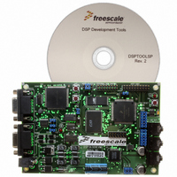
Manufacturer Part Number
DSP56309EVM
Description
KIT EVALUATION FOR XC56309
Manufacturer
Freescale Semiconductor
Type
DSPr
Specifications of DSP56309EVM
Contents
Module Board, Installation Guide, Power Supply, Cable, Software and more
Description/function
Audio DSPs
Product
Audio Modules
For Use With/related Products
DSP56309
Lead Free Status / RoHS Status
Contains lead / RoHS non-compliant


Signals/Connections
2.12 JTAG/OnCE Interface
2-20
TCK
TDI
TDO
TMS
TRST
DE
Signal Name
Input
Input
Output
Input
Input
Input/Output
Type
Input
Input
Tri-stated
Input
Input
Input
State During
Table 2-16. JTAG/OnCE Interface
Reset
DSP56309 User’s Manual, Rev. 1
Test Clock
A test clock signal for synchronizing JTAG test logic. This input is 5
V tolerant.
Test Data Input
A test data serial signal for test instructions and data. TDI is
sampled on the rising edge of TCK and has an internal pull-up
resistor. This input is 5 V tolerant.
Test Data Output
A test data serial signal for test instructions and data. TDO can be
tri-stated. The signal is actively driven in the shift-IR and shift-DR
controller states and changes on the falling edge of TCK. This pin is
5 V tolerant.
Test Mode Select
Sequences the test controller’s state machine, is sampled on the
rising edge of TCK, and has an internal pull-up resistor. This input is
5 V tolerant.
Test Reset
Asynchronously initializes the test controller, has an internal pull-up
resistor, and must be asserted after power up. This input is 5 V
tolerant.
Debug Event
Provides
controller (as input) or to acknowledge that the chip has entered
Debug mode (as output). When asserted as an input,
the DSP56300 core to finish the current instruction, save the
instruction pipeline information, enter Debug mode, and wait for
commands from the debug serial input line. When a debug request
or a breakpoint condition cause the chip to enter Debug mode
asserted as an output for three clock cycles.
pull-up resistor.
DE
Controller. It connects to the OnCE module to initiate Debug mode
directly or to provide a direct external indication that the chip has
entered the Debug mode. All other interface with the OnCE module
must occur through the JTAG port. This input is 5 V tolerant.
is not a standard part of the JTAG Test Access Port (TAP)
a way to enter Debug mode from an external command
Signal Description
Freescale Semiconductor
DE
has an internal
DE
causes
DE
is
Related parts for DSP56309EVM
Image
Part Number
Description
Manufacturer
Datasheet
Request
R

Part Number:
Description:
Manufacturer:
Freescale Semiconductor, Inc
Datasheet:
Part Number:
Description:
Manufacturer:
Freescale Semiconductor, Inc
Datasheet:
Part Number:
Description:
Manufacturer:
Freescale Semiconductor, Inc
Datasheet:
Part Number:
Description:
Manufacturer:
Freescale Semiconductor, Inc
Datasheet:
Part Number:
Description:
Manufacturer:
Freescale Semiconductor, Inc
Datasheet:
Part Number:
Description:
Manufacturer:
Freescale Semiconductor, Inc
Datasheet:
Part Number:
Description:
Manufacturer:
Freescale Semiconductor, Inc
Datasheet:
Part Number:
Description:
Manufacturer:
Freescale Semiconductor, Inc
Datasheet:
Part Number:
Description:
Manufacturer:
Freescale Semiconductor, Inc
Datasheet:
Part Number:
Description:
Manufacturer:
Freescale Semiconductor, Inc
Datasheet:
Part Number:
Description:
Manufacturer:
Freescale Semiconductor, Inc
Datasheet:
Part Number:
Description:
Manufacturer:
Freescale Semiconductor, Inc
Datasheet:
Part Number:
Description:
Manufacturer:
Freescale Semiconductor, Inc
Datasheet:
Part Number:
Description:
Manufacturer:
Freescale Semiconductor, Inc
Datasheet:
Part Number:
Description:
Manufacturer:
Freescale Semiconductor, Inc
Datasheet: