DSP56309EVM Freescale Semiconductor, DSP56309EVM Datasheet - Page 144
DSP56309EVM
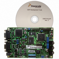
Manufacturer Part Number
DSP56309EVM
Description
KIT EVALUATION FOR XC56309
Manufacturer
Freescale Semiconductor
Type
DSPr
Specifications of DSP56309EVM
Contents
Module Board, Installation Guide, Power Supply, Cable, Software and more
Description/function
Audio DSPs
Product
Audio Modules
For Use With/related Products
DSP56309
Lead Free Status / RoHS Status
Contains lead / RoHS non-compliant


Enhanced Synchronous Serial Interface (ESSI)
7.4.9 Flags
Two ESSI signals (SC[1–0]) are available for use as serial I/O flags. Their operation is controlled
by the SYN, SCD[1–0], SSC1, and TE[2–1] bits in the CRB/CRA.The control bits OF[1–0] and
status bits IF[1–0] are double-buffered to and from SC[1–0]. Double-buffering the flags keeps
the flags in sync with TX and RX.
The SC[1–0] flags are available in Synchronous mode only. Each flag can be separately
programmed. The
direction is selected by the SCD0 bit. When SCD0 is set,
SCD0 is cleared,
is disabled (TE2 = 0), and the
signal (Bit SSC1 = 0). The direction of
SC1
When programmed as input flags, the value of the SC[1–0] bits is latched at the same time as the
first bit of the received data word is sampled. Once the input is latched, the signal on the input
flag signal (
not change until the first bit of the next data word is received. When the received data word is
latched by RX, the latched values of SC[1–0] are latched by the SSISR IF[1–0] bits, respectively,
and can be read by software.
When they are programmed as output flags, the value of the SC[1–0] bits is taken from the value
of the OF[1–0] bits. The value of OF[1–0] is latched when the contents of TX transfer to the
transmit shift register. The value on SC[1–0] is stable from the time the first bit of the transmit
data word transmits until the first bit of the next transmit data word transmits. Software can
directly set the OF[1–0] values, allowing the DSP56309 to control data transmission by indirectly
controlling the value of the SC[1–0] flags.
7.5 ESSI Programming Model
The ESSI is composed of the following registers:
7-12
is an output flag. When SCD1 is cleared,
Two control registers (CRA, CRB), page 7-13 and page 7-17
One status register (SSISR), page 7-26
One Receive Shift Register, page 7-28
One Receive Data Register (RX), page 7-28
Three Transmit Shift Registers, page 7-28
Three Transmit Data Registers (TX0, TX1, TX2), page 7-28
One special-purpose Time Slot Register (TSR), page 7-31
Two Transmit Slot Mask Registers (TSMA, TSMB), page 7-31
Two Receive Slot Mask Registers (RSMA, RSMB), page 7-32
SC0
and
SC0
SC0
SC1
is configured as input. Similarly, the
flag is enabled when transmitter 1 is disabled (TE1 = 0). The flag’s
) can change without affecting the input flag. The value of SC[1–0] does
SC1
signal is not configured as the transmitter 0 drive-enabled
DSP56309 User’s Manual, Rev. 1
SC1
is determined by the SCD1 bit. When SCD1 is set,
SC1
is an input flag.
SC0
SC1
is configured as output. When
flag is enabled when transmitter 2
Freescale Semiconductor
Related parts for DSP56309EVM
Image
Part Number
Description
Manufacturer
Datasheet
Request
R

Part Number:
Description:
Manufacturer:
Freescale Semiconductor, Inc
Datasheet:
Part Number:
Description:
Manufacturer:
Freescale Semiconductor, Inc
Datasheet:
Part Number:
Description:
Manufacturer:
Freescale Semiconductor, Inc
Datasheet:
Part Number:
Description:
Manufacturer:
Freescale Semiconductor, Inc
Datasheet:
Part Number:
Description:
Manufacturer:
Freescale Semiconductor, Inc
Datasheet:
Part Number:
Description:
Manufacturer:
Freescale Semiconductor, Inc
Datasheet:
Part Number:
Description:
Manufacturer:
Freescale Semiconductor, Inc
Datasheet:
Part Number:
Description:
Manufacturer:
Freescale Semiconductor, Inc
Datasheet:
Part Number:
Description:
Manufacturer:
Freescale Semiconductor, Inc
Datasheet:
Part Number:
Description:
Manufacturer:
Freescale Semiconductor, Inc
Datasheet:
Part Number:
Description:
Manufacturer:
Freescale Semiconductor, Inc
Datasheet:
Part Number:
Description:
Manufacturer:
Freescale Semiconductor, Inc
Datasheet:
Part Number:
Description:
Manufacturer:
Freescale Semiconductor, Inc
Datasheet:
Part Number:
Description:
Manufacturer:
Freescale Semiconductor, Inc
Datasheet:
Part Number:
Description:
Manufacturer:
Freescale Semiconductor, Inc
Datasheet: