DSP56309EVM Freescale Semiconductor, DSP56309EVM Datasheet - Page 41
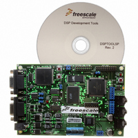
DSP56309EVM
Manufacturer Part Number
DSP56309EVM
Description
KIT EVALUATION FOR XC56309
Manufacturer
Freescale Semiconductor
Type
DSPr
Specifications of DSP56309EVM
Contents
Module Board, Installation Guide, Power Supply, Cable, Software and more
Description/function
Audio DSPs
Product
Audio Modules
For Use With/related Products
DSP56309
Lead Free Status / RoHS Status
Contains lead / RoHS non-compliant


Freescale Semiconductor
SCK1
PD3
SRD1
PD4
STD1
PD5
Notes: 1.
Signal
Name
2.
Input/Output
Input or Output
Input
Input or Output
Output
Input or Output
Table 2-13. Enhanced Synchronous Serial Interface 1 (ESSI1) (Continued)
In the Stop state, the signal maintains the last state as follows:
•
•
The Wait processing state does not affect the signal state.
Type
If the last state is input, the signal is an ignored input.
If the last state is output, these lines are tri-stated.
Ignored input
Ignored input
Ignored input
State During
Reset
1, 2
DSP56309 User’s Manual, Rev. 1
Serial Clock
Provides the serial bit rate clock for the ESSI interface for both the transmitter
and receiver in Synchronous modes, or the transmitter only in Asynchronous
modes.
Although an external serial clock can be independent of and asynchronous to
the DSP system clock, it must exceed the minimum clock cycle time of 6 T
(that is, the system clock frequency must be at least three times the external
ESSI clock frequency). The ESSI needs at least three DSP phases inside
each half of the serial clock.
Port D 3
The default configuration following reset is GPIO. For PD3, signal direction is
controlled through PRRD.
This signal is configured as SCK1 or PD3 through PCRD. This input is 5 V
tolerant.
Serial Receive Data
Receives serial data and transfers the data to the ESSI receive shift register.
SRD0 is an input when data is being received.
Port D 4
The default configuration following reset is GPIO. For PD4, signal direction is
controlled through PRRD. This signal is configured as SRD1 or PD4 through
PCRD. This input is 5 V tolerant.
Serial Transmit Data
Transmits data from the serial transmit shift register. STD1 is an output when
data is being transmitted.
Port C 5
The default configuration following reset is GPIO. For PD5, signal direction is
controlled through PRRD. This signal is configured as STD1 or PD5 through
PCRD. This input is 5 V tolerant.
Enhanced Synchronous Serial Interface 1 (ESSI1)
Signal Description
2-17
Related parts for DSP56309EVM
Image
Part Number
Description
Manufacturer
Datasheet
Request
R

Part Number:
Description:
Manufacturer:
Freescale Semiconductor, Inc
Datasheet:
Part Number:
Description:
Manufacturer:
Freescale Semiconductor, Inc
Datasheet:
Part Number:
Description:
Manufacturer:
Freescale Semiconductor, Inc
Datasheet:
Part Number:
Description:
Manufacturer:
Freescale Semiconductor, Inc
Datasheet:
Part Number:
Description:
Manufacturer:
Freescale Semiconductor, Inc
Datasheet:
Part Number:
Description:
Manufacturer:
Freescale Semiconductor, Inc
Datasheet:
Part Number:
Description:
Manufacturer:
Freescale Semiconductor, Inc
Datasheet:
Part Number:
Description:
Manufacturer:
Freescale Semiconductor, Inc
Datasheet:
Part Number:
Description:
Manufacturer:
Freescale Semiconductor, Inc
Datasheet:
Part Number:
Description:
Manufacturer:
Freescale Semiconductor, Inc
Datasheet:
Part Number:
Description:
Manufacturer:
Freescale Semiconductor, Inc
Datasheet:
Part Number:
Description:
Manufacturer:
Freescale Semiconductor, Inc
Datasheet:
Part Number:
Description:
Manufacturer:
Freescale Semiconductor, Inc
Datasheet:
Part Number:
Description:
Manufacturer:
Freescale Semiconductor, Inc
Datasheet:
Part Number:
Description:
Manufacturer:
Freescale Semiconductor, Inc
Datasheet: