DSP56309EVM Freescale Semiconductor, DSP56309EVM Datasheet - Page 29
DSP56309EVM
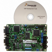
Manufacturer Part Number
DSP56309EVM
Description
KIT EVALUATION FOR XC56309
Manufacturer
Freescale Semiconductor
Type
DSPr
Specifications of DSP56309EVM
Contents
Module Board, Installation Guide, Power Supply, Cable, Software and more
Description/function
Audio DSPs
Product
Audio Modules
For Use With/related Products
DSP56309
Lead Free Status / RoHS Status
Contains lead / RoHS non-compliant


2.4 Phase Lock Loop (PLL)
2.5 External Memory Expansion Port (Port A)
Note:
2.5.1 External Address Bus
Freescale Semiconductor
A[0–17]
PCAP
CLKOUT
PINIT/NMI
Signal Name
Signal
Name
When the DSP56309 enters a low-power standby mode (Stop or Wait), it releases bus
mastership and tri-states the relevant Port A signals:
AA0
Output
Type
/
RAS0
Input
Output
Input
Type
–
AA3
Tri-stated
State During Reset,
/
Input
Chip-driven
Input
RAS3
Stop, or Wait
State During
Table 2-6. External Address Bus Signals
Reset
Table 2-5. Phase Lock Loop Signals
,
RD
,
DSP56309 User’s Manual, Rev. 1
WR
,
PLL Capacitor
Connects an off-chip capacitor to the PLL filter. See the DSP56309
Technical Data sheet to determine the correct PLL capacitor value.
Connect one capacitor terminal to PCAP and the other terminal to V
If the PLL is not used, PCAP can be tied to V
Clock Output
Provides an output clock synchronized to the internal core clock phase.
If the PLL is enabled and both the multiplication and division factors
equal one, then CLKOUT is also synchronized to EXTAL.
If the PLL is disabled, the CLKOUT frequency is half the frequency of
EXTAL.
PLL Initial/Non-Maskable Interrupt
During assertion of RESET, the value of PINIT/NMI is written into the PLL
Enable (PEN) bit of the PLL control register, determining whether the
PLL is enabled or disabled. After RESET deassertion and during normal
instruction processing, the PINIT/
negative-edge-triggered Non-Maskable Interrupt (NMI) request internally
synchronized to CLKOUT.
PINIT/NMI can tolerate 5 V.
BB
,
Address Bus
When the DSP is the bus master, A[0–17] specify the address for
external program and data memory accesses. Otherwise, the signals
are tri-stated. To minimize power dissipation, A[0–17] do not change
state when external memory spaces are not being accessed.
CAS
,
BCLK
,
BCLK
Signal Description
.
Signal Description
A[0–17]
NMI
Schmitt-trigger input is a
,
D[0–23]
CC
, GND, or left floating.
Phase Lock Loop (PLL)
,
CCP
2-5
.
Related parts for DSP56309EVM
Image
Part Number
Description
Manufacturer
Datasheet
Request
R

Part Number:
Description:
Manufacturer:
Freescale Semiconductor, Inc
Datasheet:
Part Number:
Description:
Manufacturer:
Freescale Semiconductor, Inc
Datasheet:
Part Number:
Description:
Manufacturer:
Freescale Semiconductor, Inc
Datasheet:
Part Number:
Description:
Manufacturer:
Freescale Semiconductor, Inc
Datasheet:
Part Number:
Description:
Manufacturer:
Freescale Semiconductor, Inc
Datasheet:
Part Number:
Description:
Manufacturer:
Freescale Semiconductor, Inc
Datasheet:
Part Number:
Description:
Manufacturer:
Freescale Semiconductor, Inc
Datasheet:
Part Number:
Description:
Manufacturer:
Freescale Semiconductor, Inc
Datasheet:
Part Number:
Description:
Manufacturer:
Freescale Semiconductor, Inc
Datasheet:
Part Number:
Description:
Manufacturer:
Freescale Semiconductor, Inc
Datasheet:
Part Number:
Description:
Manufacturer:
Freescale Semiconductor, Inc
Datasheet:
Part Number:
Description:
Manufacturer:
Freescale Semiconductor, Inc
Datasheet:
Part Number:
Description:
Manufacturer:
Freescale Semiconductor, Inc
Datasheet:
Part Number:
Description:
Manufacturer:
Freescale Semiconductor, Inc
Datasheet:
Part Number:
Description:
Manufacturer:
Freescale Semiconductor, Inc
Datasheet: