DSP56309EVM Freescale Semiconductor, DSP56309EVM Datasheet - Page 137
DSP56309EVM
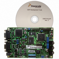
Manufacturer Part Number
DSP56309EVM
Description
KIT EVALUATION FOR XC56309
Manufacturer
Freescale Semiconductor
Type
DSPr
Specifications of DSP56309EVM
Contents
Module Board, Installation Guide, Power Supply, Cable, Software and more
Description/function
Audio DSPs
Product
Audio Modules
For Use With/related Products
DSP56309
Lead Free Status / RoHS Status
Contains lead / RoHS non-compliant


When configured as an output,
drive-enabled signal, or as the receive frame sync signal output. If
Flag 1, its value is determined by the value of the serial Output Flag 1 (OF1) bit in the CRB.
When configured as an input, this signal can receive frame sync signals from an external source,
or it acts as a serial input flag. As a serial input flag, SC1controls status bit IF1 in the SSISR.
When
SCD1 bit value. As an output, it is fully synchronized with the other ESSI transmit data signals
(
in use.
7.2.6 Serial Control Signal (SC2)
ESSI0:SC02; ESSI1:SC12
SC2
the transmitter only in Asynchronous mode. The direction of this signal is determined by the
SCD2 bit in the CRB. When configured as an output, this signal outputs the internally generated
frame sync signal. When configured as an input, this signal receives an external frame sync signal
for the transmitter in Asynchronous mode and for both the transmitter and receiver when in
Synchronous mode.
not in use.
Freescale Semiconductor
STD
TXC
RXC
XC
FST
FSR
FS
TD0
TD1
TD2
T0D
RD
F0
F1
U
X
SYN
1
1
1
1
1
1
1
is a frame sync I/O signal for both the transmitter and receiver in Synchronous mode and for
and
SC1
=
=
=
=
=
=
=
=
=
=
=
=
=
=
=
SC0
TE0
is configured as a transmit data signal, it is always an output signal, regardless of the
1
1
1
1
1
1
1
Indeterminate
Transmitter clock
Receiver clock
Transmitter/receiver clock (synchronous operation)
Transmitter frame sync
Receiver frame sync
Transmitter/receiver frame sync (synchronous operation)
Transmit data signal 0
Transmit data signal 1
Transmit data signal 2
Transmitter 0 drive enable if SSC1 = 1 & SCD1 = 1
Receive data
Flag 0
Flag 1 if SSC1 = 0
Unused (can be used as GPIO signal)
).
Control Bits
SC1
TE1
0
0
0
1
1
1
1
can be programmed as a GPIO signal (P1) when the ESSI
SC2
Table 7-2. Mode and Signal Definitions (Continued)
can be programmed as a GPIO signal (
TE2
0
1
1
0
0
1
1
SC1
RE
1
0
1
0
1
0
1
DSP56309 User’s Manual, Rev. 1
functions as a serial Output Flag, as the transmitter 0
F0/U
F0/U
F0/U
SC0
TD1
TD1
TD1
TD1
F1/T0D/U
F1/T0D/U
F1/T0D/U
SC1
TD2
TD2
TD2
TD2
P2
ESSI Signals
SC2
) when the ESSI
FS
FS
FS
FS
FS
FS
FS
SC1
is used as serial Output
ESSI Data and Control Signals
SCK
XC
XC
XC
XC
XC
XC
XC
SC1
SC2
function is not
STD
TD0
TD0
TD0
TD0
TD0
TD0
TD0
function is
SRD
RD
RD
RD
RD
U
U
U
7-5
Related parts for DSP56309EVM
Image
Part Number
Description
Manufacturer
Datasheet
Request
R

Part Number:
Description:
Manufacturer:
Freescale Semiconductor, Inc
Datasheet:
Part Number:
Description:
Manufacturer:
Freescale Semiconductor, Inc
Datasheet:
Part Number:
Description:
Manufacturer:
Freescale Semiconductor, Inc
Datasheet:
Part Number:
Description:
Manufacturer:
Freescale Semiconductor, Inc
Datasheet:
Part Number:
Description:
Manufacturer:
Freescale Semiconductor, Inc
Datasheet:
Part Number:
Description:
Manufacturer:
Freescale Semiconductor, Inc
Datasheet:
Part Number:
Description:
Manufacturer:
Freescale Semiconductor, Inc
Datasheet:
Part Number:
Description:
Manufacturer:
Freescale Semiconductor, Inc
Datasheet:
Part Number:
Description:
Manufacturer:
Freescale Semiconductor, Inc
Datasheet:
Part Number:
Description:
Manufacturer:
Freescale Semiconductor, Inc
Datasheet:
Part Number:
Description:
Manufacturer:
Freescale Semiconductor, Inc
Datasheet:
Part Number:
Description:
Manufacturer:
Freescale Semiconductor, Inc
Datasheet:
Part Number:
Description:
Manufacturer:
Freescale Semiconductor, Inc
Datasheet:
Part Number:
Description:
Manufacturer:
Freescale Semiconductor, Inc
Datasheet:
Part Number:
Description:
Manufacturer:
Freescale Semiconductor, Inc
Datasheet: