C8051F930-TB Silicon Laboratories Inc, C8051F930-TB Datasheet - Page 90
C8051F930-TB
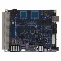
Manufacturer Part Number
C8051F930-TB
Description
BOARD TARGET/PROTO W/C8051F930
Manufacturer
Silicon Laboratories Inc
Type
MCUr
Specifications of C8051F930-TB
Contents
Board
Processor To Be Evaluated
C8051F930
Processor Series
C8051F9xx
Data Bus Width
8 bit
Interface Type
I2C, UART, SPI
Maximum Operating Temperature
+ 85 C
Minimum Operating Temperature
- 40 C
Operating Supply Voltage
0.9 V to 3.6 V
Lead Free Status / RoHS Status
Lead free / RoHS Compliant
For Use With/related Products
C8051F930
Lead Free Status / Rohs Status
Lead free / RoHS Compliant
Other names
336-1472


C8051F93x-C8051F92x
7.
C8051F93x-C8051F92x devices include two on-chip programmable voltage comparators: Comparator 0
(CPT0) is shown in Figure 7.1; Comparator 1 (CPT1) is shown in Figure 7.2. The two comparators operate
identically, but may differ in their ability to be used as reset or wake-up sources. See the Reset Sources
chapter and the Power Management chapter for details on reset sources and low power mode wake-up
sources, respectively.
The Comparator offers programmable response time and hysteresis, an analog input multiplexer, and two
outputs that are optionally available at the Port pins: a synchronous “latched” output (CP0, CP1), or an
asynchronous “raw” output (CP0A, CP1A). The asynchronous CP0A signal is available even when the
system clock is not active. This allows the Comparator to operate and generate an output when the device
is in some low power modes.
7.1.
Each Comparator performs an analog comparison of the voltage levels at its positive (CP0+ or CP1+) and
negative (CP0- or CP1-) input. Both comparators support multiple port pin inputs multiplexed to their posi-
tive and negative comparator inputs using analog input multiplexers. The analog input multiplexers are
completely under software control and configured using SFR registers. See Section “7.6. Comparator0 and
Comparator1 Analog Multiplexers” on page 97 for details on how to select and configure Comparator
inputs.
Important Note About Comparator Inputs: The Port pins selected as Comparator inputs should be con-
figured as analog inputs and skipped by the Crossbar. See the Port I/O chapter for more details on how to
configure Port I/O pins as Analog Inputs. The Comparator may also be used to compare the logic level of
digital signals, however, Port I/O pins configured as digital inputs must be driven to a valid logic state
(HIGH or LOW) to avoid increased power consumption.
90
Comparators
Analog Input Multiplexer
Px.x
Px.x
Px.x
Px.x
Comparator Inputs
Figure 7.1. Comparator 0 Functional Block Diagram
CP0HYN1
CP0HYN0
CP0HYP1
CP0HYP0
CP0OUT
CP0RIF
CP0FIF
CP0EN
CP0 +
CP0 -
+
-
Rev. 1.1
VDD
GND
Decision
Reset
CPT0MD
Tree
(ASYNCHRONOUS)
(SYNCHRONIZER)
D
SET
CLR
Q
Q
D
SET
CLR
Q
Q
Rising-edge
CP0
Crossbar
Interrupt
Logic
Falling-edge
Interrupt
CP0
CP0A
CP0
CP0
Related parts for C8051F930-TB
Image
Part Number
Description
Manufacturer
Datasheet
Request
R

Part Number:
Description:
SMD/C°/SINGLE-ENDED OUTPUT SILICON OSCILLATOR
Manufacturer:
Silicon Laboratories Inc
Part Number:
Description:
Manufacturer:
Silicon Laboratories Inc
Datasheet:
Part Number:
Description:
N/A N/A/SI4010 AES KEYFOB DEMO WITH LCD RX
Manufacturer:
Silicon Laboratories Inc
Datasheet:
Part Number:
Description:
N/A N/A/SI4010 SIMPLIFIED KEY FOB DEMO WITH LED RX
Manufacturer:
Silicon Laboratories Inc
Datasheet:
Part Number:
Description:
N/A/-40 TO 85 OC/EZLINK MODULE; F930/4432 HIGH BAND (REV E/B1)
Manufacturer:
Silicon Laboratories Inc
Part Number:
Description:
EZLink Module; F930/4432 Low Band (rev e/B1)
Manufacturer:
Silicon Laboratories Inc
Part Number:
Description:
I°/4460 10 DBM RADIO TEST CARD 434 MHZ
Manufacturer:
Silicon Laboratories Inc
Part Number:
Description:
I°/4461 14 DBM RADIO TEST CARD 868 MHZ
Manufacturer:
Silicon Laboratories Inc
Part Number:
Description:
I°/4463 20 DBM RFSWITCH RADIO TEST CARD 460 MHZ
Manufacturer:
Silicon Laboratories Inc
Part Number:
Description:
I°/4463 20 DBM RADIO TEST CARD 868 MHZ
Manufacturer:
Silicon Laboratories Inc
Part Number:
Description:
I°/4463 27 DBM RADIO TEST CARD 868 MHZ
Manufacturer:
Silicon Laboratories Inc
Part Number:
Description:
I°/4463 SKYWORKS 30 DBM RADIO TEST CARD 915 MHZ
Manufacturer:
Silicon Laboratories Inc
Part Number:
Description:
N/A N/A/-40 TO 85 OC/4463 RFMD 30 DBM RADIO TEST CARD 915 MHZ
Manufacturer:
Silicon Laboratories Inc
Part Number:
Description:
I°/4463 20 DBM RADIO TEST CARD 169 MHZ
Manufacturer:
Silicon Laboratories Inc