C8051F930-TB Silicon Laboratories Inc, C8051F930-TB Datasheet - Page 178
C8051F930-TB
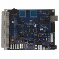
Manufacturer Part Number
C8051F930-TB
Description
BOARD TARGET/PROTO W/C8051F930
Manufacturer
Silicon Laboratories Inc
Type
MCUr
Specifications of C8051F930-TB
Contents
Board
Processor To Be Evaluated
C8051F930
Processor Series
C8051F9xx
Data Bus Width
8 bit
Interface Type
I2C, UART, SPI
Maximum Operating Temperature
+ 85 C
Minimum Operating Temperature
- 40 C
Operating Supply Voltage
0.9 V to 3.6 V
Lead Free Status / RoHS Status
Lead free / RoHS Compliant
For Use With/related Products
C8051F930
Lead Free Status / Rohs Status
Lead free / RoHS Compliant
Other names
336-1472


C8051F93x-C8051F92x
SFR Definition 16.2. DC0CF: DC-DC Converter Configuration
SFR Page = 0x0; SFR Address = 0x96
16.10. DC-DC Converter Specifications
See Table 4.14 on page 64 for a detailed listing of dc-dc converter specifications.
178
Reset
Name Reserved
Type
Bit
6:5 CLKDIV[1:0] DC
7
4
3
2
1
0
Bit
AD0CKINV ADC0 Clock Inversion (Clock Invert During Sync).
Reserved
VDDSLP
CLKSEL
CLKINV
ILIMIT
Name
R
7
0
Reserved.
Read = 0b; Must write 0b.
Divides the dc-dc converter clock when the system clock is selected as the clock
source for dc-dc converter. These bits are ignored when the dc-dc converter is
clocked from its local oscillator.
00: The dc-dc converter clock is system clock divided by 1.
01: The dc-dc converter clock is system clock divided by 2.
10: The dc-dc converter clock is system clock divided by 4.
11: The dc-dc converter clock is system clock divided by 8.
Inverts the ADC0 SAR clock derived from the dc-dc converter clock when the SYNC
bit (DC0CN.3) is enabled. This bit is ignored when the SYNC bit is set to zero.
0: ADC0 SAR clock is inverted.
1: ADC0 SAR clock is not inverted.
DC
Inverts the system clock used as the input to the dc-dc clock divider.
0: The dc-dc converter clock is not inverted.
1: The dc-dc converter clock is inverted.
Peak Current Limit Threshold.
Sets the threshold for the maximum allowed peak inductor current. See Table 16.1
for peak inductor current levels.
0: Peak inductor current is set at a lower level.
1: Peak inductor current is set at a higher level.
VDD
Specifies the power source for VDD/DC+ in Sleep Mode when the dc-dc converter is
enabled.
0: VDD-DC+ connected to VBAT in Sleep Mode.
1: VDD-DC+ is floating in Sleep Mode.
DC
Specifies the dc-dc converter clock source.
0: The dc-dc converter is clocked from its local oscillator.
1: The dc-dc converter is clocked from the system clock.
R/W
-
-
-
DC Clock Divider.
DC Converter Clock Invert.
DC Converter Clock Source Select.
0
-
6
CLKDIV[1:0]
DC+ Sleep Mode Connection.
R/W
5
0
AD0CKINV
Rev. 1.1
R/W
4
0
Function
CLKINV
R/W
3
0
ILIMIT
R/W
2
0
VDDSLP
R/W
1
0
CLKSEL
R/W
0
0
Related parts for C8051F930-TB
Image
Part Number
Description
Manufacturer
Datasheet
Request
R

Part Number:
Description:
SMD/C°/SINGLE-ENDED OUTPUT SILICON OSCILLATOR
Manufacturer:
Silicon Laboratories Inc
Part Number:
Description:
Manufacturer:
Silicon Laboratories Inc
Datasheet:
Part Number:
Description:
N/A N/A/SI4010 AES KEYFOB DEMO WITH LCD RX
Manufacturer:
Silicon Laboratories Inc
Datasheet:
Part Number:
Description:
N/A N/A/SI4010 SIMPLIFIED KEY FOB DEMO WITH LED RX
Manufacturer:
Silicon Laboratories Inc
Datasheet:
Part Number:
Description:
N/A/-40 TO 85 OC/EZLINK MODULE; F930/4432 HIGH BAND (REV E/B1)
Manufacturer:
Silicon Laboratories Inc
Part Number:
Description:
EZLink Module; F930/4432 Low Band (rev e/B1)
Manufacturer:
Silicon Laboratories Inc
Part Number:
Description:
I°/4460 10 DBM RADIO TEST CARD 434 MHZ
Manufacturer:
Silicon Laboratories Inc
Part Number:
Description:
I°/4461 14 DBM RADIO TEST CARD 868 MHZ
Manufacturer:
Silicon Laboratories Inc
Part Number:
Description:
I°/4463 20 DBM RFSWITCH RADIO TEST CARD 460 MHZ
Manufacturer:
Silicon Laboratories Inc
Part Number:
Description:
I°/4463 20 DBM RADIO TEST CARD 868 MHZ
Manufacturer:
Silicon Laboratories Inc
Part Number:
Description:
I°/4463 27 DBM RADIO TEST CARD 868 MHZ
Manufacturer:
Silicon Laboratories Inc
Part Number:
Description:
I°/4463 SKYWORKS 30 DBM RADIO TEST CARD 915 MHZ
Manufacturer:
Silicon Laboratories Inc
Part Number:
Description:
N/A N/A/-40 TO 85 OC/4463 RFMD 30 DBM RADIO TEST CARD 915 MHZ
Manufacturer:
Silicon Laboratories Inc
Part Number:
Description:
I°/4463 20 DBM RADIO TEST CARD 169 MHZ
Manufacturer:
Silicon Laboratories Inc