C8051F930-TB Silicon Laboratories Inc, C8051F930-TB Datasheet - Page 128
C8051F930-TB
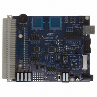
Manufacturer Part Number
C8051F930-TB
Description
BOARD TARGET/PROTO W/C8051F930
Manufacturer
Silicon Laboratories Inc
Type
MCUr
Specifications of C8051F930-TB
Contents
Board
Processor To Be Evaluated
C8051F930
Processor Series
C8051F9xx
Data Bus Width
8 bit
Interface Type
I2C, UART, SPI
Maximum Operating Temperature
+ 85 C
Minimum Operating Temperature
- 40 C
Operating Supply Voltage
0.9 V to 3.6 V
Lead Free Status / RoHS Status
Lead free / RoHS Compliant
For Use With/related Products
C8051F930
Lead Free Status / Rohs Status
Lead free / RoHS Compliant
Other names
336-1472


C8051F93x-C8051F92x
SFR Definition 11.1. SFR Page: SFR Page
SFR Page = All Pages; SFR Address = 0xA7
128
SFRs are listed in alphabetical order. All undefined SFR locations are reserved
Register
ACC
ADC0AC
ADC0CF
ADC0CN
ADC0GTH
ADC0GTL
ADC0H
ADC0L
ADC0LTH
ADC0LTL
ADC0MX
ADC0PWR
ADC0TK
B
CKCON
CLKSEL
CPT0CN
CPT0MD
CPT0MX
CPT1CN
Reset
Name
Bit
7:0 SFRPAGE[7:0] SFR Page.
Type
Bit
Name
7
0
Address
0xBA
0xBC
0xC4
0xC3
0xBE
0xBD
0xC6
0xC5
0xBB
0xBA
0xBD
0x9D
0xE0
0xE8
0xF0
0x8E
0xA9
0x9B
0x9F
0x9A
Specifies the SFR Page used when reading, writing, or modifying special function
registers.
0
6
Table 11.3. Special Function Registers
SFR Page
0x0
0x0
0x0
0x0
0x0
0x0
0x0
0x0
0x0
0x0
0xF
0xF
0x0
0x0
0x0
0x0
0x0
All
All
All
5
0
Accumulator
ADC0 Accumulator Configuration
ADC0 Configuration
ADC0 Control
ADC0 Greater-Than Compare High
ADC0 Greater-Than Compare Low
ADC0 High
ADC0 Low
ADC0 Less-Than Compare Word High
ADC0 Less-Than Compare Word Low
AMUX0 Channel Select
ADC0 Burst Mode Power-Up Time
ADC0 Tracking Control
B Register
Clock Control
Clock Select
Comparator0 Control
Comparator0 Mode Selection
Comparator0 Mux Selection
Comparator1 Control
Rev. 1.1
SFRPAGE[7:0]
4
0
R/W
Function
3
0
Description
2
0
1
0
0
0
Page
107
107
279
193
74
73
72
78
78
77
77
79
79
82
75
76
94
94
98
95
Related parts for C8051F930-TB
Image
Part Number
Description
Manufacturer
Datasheet
Request
R

Part Number:
Description:
SMD/C°/SINGLE-ENDED OUTPUT SILICON OSCILLATOR
Manufacturer:
Silicon Laboratories Inc
Part Number:
Description:
Manufacturer:
Silicon Laboratories Inc
Datasheet:
Part Number:
Description:
N/A N/A/SI4010 AES KEYFOB DEMO WITH LCD RX
Manufacturer:
Silicon Laboratories Inc
Datasheet:
Part Number:
Description:
N/A N/A/SI4010 SIMPLIFIED KEY FOB DEMO WITH LED RX
Manufacturer:
Silicon Laboratories Inc
Datasheet:
Part Number:
Description:
N/A/-40 TO 85 OC/EZLINK MODULE; F930/4432 HIGH BAND (REV E/B1)
Manufacturer:
Silicon Laboratories Inc
Part Number:
Description:
EZLink Module; F930/4432 Low Band (rev e/B1)
Manufacturer:
Silicon Laboratories Inc
Part Number:
Description:
I°/4460 10 DBM RADIO TEST CARD 434 MHZ
Manufacturer:
Silicon Laboratories Inc
Part Number:
Description:
I°/4461 14 DBM RADIO TEST CARD 868 MHZ
Manufacturer:
Silicon Laboratories Inc
Part Number:
Description:
I°/4463 20 DBM RFSWITCH RADIO TEST CARD 460 MHZ
Manufacturer:
Silicon Laboratories Inc
Part Number:
Description:
I°/4463 20 DBM RADIO TEST CARD 868 MHZ
Manufacturer:
Silicon Laboratories Inc
Part Number:
Description:
I°/4463 27 DBM RADIO TEST CARD 868 MHZ
Manufacturer:
Silicon Laboratories Inc
Part Number:
Description:
I°/4463 SKYWORKS 30 DBM RADIO TEST CARD 915 MHZ
Manufacturer:
Silicon Laboratories Inc
Part Number:
Description:
N/A N/A/-40 TO 85 OC/4463 RFMD 30 DBM RADIO TEST CARD 915 MHZ
Manufacturer:
Silicon Laboratories Inc
Part Number:
Description:
I°/4463 20 DBM RADIO TEST CARD 169 MHZ
Manufacturer:
Silicon Laboratories Inc