C8051F930-TB Silicon Laboratories Inc, C8051F930-TB Datasheet - Page 87
C8051F930-TB
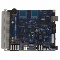
Manufacturer Part Number
C8051F930-TB
Description
BOARD TARGET/PROTO W/C8051F930
Manufacturer
Silicon Laboratories Inc
Type
MCUr
Specifications of C8051F930-TB
Contents
Board
Processor To Be Evaluated
C8051F930
Processor Series
C8051F9xx
Data Bus Width
8 bit
Interface Type
I2C, UART, SPI
Maximum Operating Temperature
+ 85 C
Minimum Operating Temperature
- 40 C
Operating Supply Voltage
0.9 V to 3.6 V
Lead Free Status / RoHS Status
Lead free / RoHS Compliant
For Use With/related Products
C8051F930
Lead Free Status / Rohs Status
Lead free / RoHS Compliant
Other names
336-1472


5.8.
To use an external voltage reference, REFSL[1:0] should be set to 00 and the internal 1.68 V precision ref-
erence should be disabled by setting REFOE to 0. Bypass capacitors should be added as recommended
by the manufacturer of the external voltage reference.
5.9.
For applications requiring the maximum number of port I/O pins, or very short VREF turn-on time, the
1.65 V high-speed reference will be the best internal reference option to choose. The high speed internal
reference is selected by setting REFSL[1:0] to 11. When selected, the high speed internal reference will be
automatically enabled/disabled on an as-needed basis by ADC0.
For applications requiring the highest absolute accuracy, the 1.68 V precision voltage reference will be the
best internal reference option to choose. The 1.68 V precision reference may be enabled and selected by
setting REFOE to 1 and REFSL[1:0] to 00. An external capacitor of at least 0.1 µF is recommended when
using the precision voltage reference.
In applications that leave the precision internal oscillator always running, there is no additional power
required to use the precision voltage reference. In all other applications, using the high speed reference
will result in lower overall power consumption due to its minimal startup time and the fact that it remains in
a low power state when an ADC conversion is not taking place.
Note: When using the precision internal oscillator as the system clock source, the precision volt-
age reference should not be enabled from a disabled state. To use the precision oscillator and the
precision voltage reference simultaneously, the precision voltage reference should be enabled first
and allowed to settle to its final value (charging the external capacitor) before the precision oscilla-
tor is started and selected as the system clock.
For applications with a non-varying power supply voltage, using the power supply as the voltage reference
can provide ADC0 with added dynamic range at the cost of reduced power supply noise rejection. To use
the 1.8 to 3.6 V power supply voltage (V
ence source, REFSL[1:0] should be set to 01 or 10, respectively.
5.10. Analog Ground Reference
To prevent ground noise generated by switching digital logic from affecting sensitive analog measure-
ments, a separate analog ground reference option is available. When enabled, the ground reference for
ADC0 during both the tracking/sampling and the conversion periods is taken from the P0.1/AGND pin. Any
external sensors sampled by ADC0 should be referenced to the P0.1/AGND pin. This pin should be con-
nected to the ground terminal of any external sensors sampled by ADC0. If an external voltage reference is
used, the P0.1/AGND pin should be connected to the ground of the external reference and its associated
decoupling capacitor. If the 1.68 V precision internal reference is used, then P0.1/AGND should be con-
nected to the ground terminal of its external decoupling capacitor. The separate analog ground reference
option is enabled by setting REFGND to 1. Note that when sampling the internal temperature sensor, the
internal chip ground is always used for the sampling operation, regardless of the setting of the REFGND
bit. Similarly, whenever the internal 1.65 V high-speed reference is selected, the internal chip ground is
always used during the conversion period, regardless of the setting of the REFGND bit.
5.11. Temperature Sensor Enable
The TEMPE bit in register REF0CN enables/disables the temperature sensor. While disabled, the temper-
ature sensor defaults to a high impedance state and any ADC0 measurements performed on the sensor
result in meaningless data. See Section “5.6. Temperature Sensor” on page 83 for details on temperature
sensor characteristics when it is enabled.
External Voltage References
Internal Voltage References
DD
/DC+) or the 1.8 V regulated digital supply voltage as the refer-
Rev. 1.1
C8051F93x-C8051F92x
87
Related parts for C8051F930-TB
Image
Part Number
Description
Manufacturer
Datasheet
Request
R

Part Number:
Description:
SMD/C°/SINGLE-ENDED OUTPUT SILICON OSCILLATOR
Manufacturer:
Silicon Laboratories Inc
Part Number:
Description:
Manufacturer:
Silicon Laboratories Inc
Datasheet:
Part Number:
Description:
N/A N/A/SI4010 AES KEYFOB DEMO WITH LCD RX
Manufacturer:
Silicon Laboratories Inc
Datasheet:
Part Number:
Description:
N/A N/A/SI4010 SIMPLIFIED KEY FOB DEMO WITH LED RX
Manufacturer:
Silicon Laboratories Inc
Datasheet:
Part Number:
Description:
N/A/-40 TO 85 OC/EZLINK MODULE; F930/4432 HIGH BAND (REV E/B1)
Manufacturer:
Silicon Laboratories Inc
Part Number:
Description:
EZLink Module; F930/4432 Low Band (rev e/B1)
Manufacturer:
Silicon Laboratories Inc
Part Number:
Description:
I°/4460 10 DBM RADIO TEST CARD 434 MHZ
Manufacturer:
Silicon Laboratories Inc
Part Number:
Description:
I°/4461 14 DBM RADIO TEST CARD 868 MHZ
Manufacturer:
Silicon Laboratories Inc
Part Number:
Description:
I°/4463 20 DBM RFSWITCH RADIO TEST CARD 460 MHZ
Manufacturer:
Silicon Laboratories Inc
Part Number:
Description:
I°/4463 20 DBM RADIO TEST CARD 868 MHZ
Manufacturer:
Silicon Laboratories Inc
Part Number:
Description:
I°/4463 27 DBM RADIO TEST CARD 868 MHZ
Manufacturer:
Silicon Laboratories Inc
Part Number:
Description:
I°/4463 SKYWORKS 30 DBM RADIO TEST CARD 915 MHZ
Manufacturer:
Silicon Laboratories Inc
Part Number:
Description:
N/A N/A/-40 TO 85 OC/4463 RFMD 30 DBM RADIO TEST CARD 915 MHZ
Manufacturer:
Silicon Laboratories Inc
Part Number:
Description:
I°/4463 20 DBM RADIO TEST CARD 169 MHZ
Manufacturer:
Silicon Laboratories Inc