C8051F930-TB Silicon Laboratories Inc, C8051F930-TB Datasheet - Page 263
C8051F930-TB
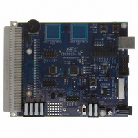
Manufacturer Part Number
C8051F930-TB
Description
BOARD TARGET/PROTO W/C8051F930
Manufacturer
Silicon Laboratories Inc
Type
MCUr
Specifications of C8051F930-TB
Contents
Board
Processor To Be Evaluated
C8051F930
Processor Series
C8051F9xx
Data Bus Width
8 bit
Interface Type
I2C, UART, SPI
Maximum Operating Temperature
+ 85 C
Minimum Operating Temperature
- 40 C
Operating Supply Voltage
0.9 V to 3.6 V
Lead Free Status / RoHS Status
Lead free / RoHS Compliant
For Use With/related Products
C8051F930
Lead Free Status / Rohs Status
Lead free / RoHS Compliant
Other names
336-1472


24. Enhanced Serial Peripheral Interface (SPI0 and SPI1)
The Enhanced Serial Peripheral Interfaces (SPI0 and SPI1) provide access to two identical, flexible, full-
duplex synchronous serial busses. Both SPI0 and SPI1 will be referred to collectively as SPIn. SPIn can
operate as a master or slave device in both 3-wire or 4-wire modes, and supports multiple masters and
slaves on a single SPI bus. The slave-select (NSS) signal can be configured as an input to select SPIn in
slave mode, or to disable Master Mode operation in a multi-master environment, avoiding contention on
the SPI bus when more than one master attempts simultaneous data transfers. NSS can also be
configured as a chip-select output in master mode, or disabled for 3-wire operation. Additional general
purpose port I/O pins can be used to select multiple slave devices in master mode.
SYSCLK
Clock Divide
SPInCKR
SFR Bus
SPI0DAT
Logic
Write
Transmit Data Buffer
Receive Data Buffer
7
Figure 24.1. SPI Block Diagram
6
Shift Register
5
SPI CONTROL LOGIC
4
3
Data Path
2
SFR Bus
Control
SPInCFG
SPInDAT
1
SPI0DAT
Read
0
Rev. 1.1
Tx Data
Rx Data
Pin Interface
C8051F93x-C8051F92x
Control
Control
Logic
Pin
SPInCN
MOSI
MISO
SCK
NSS
C
R
O
S
S
B
A
R
SPIn IRQ
Port I/O
263
Related parts for C8051F930-TB
Image
Part Number
Description
Manufacturer
Datasheet
Request
R

Part Number:
Description:
SMD/C°/SINGLE-ENDED OUTPUT SILICON OSCILLATOR
Manufacturer:
Silicon Laboratories Inc
Part Number:
Description:
Manufacturer:
Silicon Laboratories Inc
Datasheet:
Part Number:
Description:
N/A N/A/SI4010 AES KEYFOB DEMO WITH LCD RX
Manufacturer:
Silicon Laboratories Inc
Datasheet:
Part Number:
Description:
N/A N/A/SI4010 SIMPLIFIED KEY FOB DEMO WITH LED RX
Manufacturer:
Silicon Laboratories Inc
Datasheet:
Part Number:
Description:
N/A/-40 TO 85 OC/EZLINK MODULE; F930/4432 HIGH BAND (REV E/B1)
Manufacturer:
Silicon Laboratories Inc
Part Number:
Description:
EZLink Module; F930/4432 Low Band (rev e/B1)
Manufacturer:
Silicon Laboratories Inc
Part Number:
Description:
I°/4460 10 DBM RADIO TEST CARD 434 MHZ
Manufacturer:
Silicon Laboratories Inc
Part Number:
Description:
I°/4461 14 DBM RADIO TEST CARD 868 MHZ
Manufacturer:
Silicon Laboratories Inc
Part Number:
Description:
I°/4463 20 DBM RFSWITCH RADIO TEST CARD 460 MHZ
Manufacturer:
Silicon Laboratories Inc
Part Number:
Description:
I°/4463 20 DBM RADIO TEST CARD 868 MHZ
Manufacturer:
Silicon Laboratories Inc
Part Number:
Description:
I°/4463 27 DBM RADIO TEST CARD 868 MHZ
Manufacturer:
Silicon Laboratories Inc
Part Number:
Description:
I°/4463 SKYWORKS 30 DBM RADIO TEST CARD 915 MHZ
Manufacturer:
Silicon Laboratories Inc
Part Number:
Description:
N/A N/A/-40 TO 85 OC/4463 RFMD 30 DBM RADIO TEST CARD 915 MHZ
Manufacturer:
Silicon Laboratories Inc
Part Number:
Description:
I°/4463 20 DBM RADIO TEST CARD 169 MHZ
Manufacturer:
Silicon Laboratories Inc