DK-DEV-2AGX125N Altera, DK-DEV-2AGX125N Datasheet - Page 9
DK-DEV-2AGX125N
Manufacturer Part Number
DK-DEV-2AGX125N
Description
KIT DEV ARRIA II GX FPGA 2AGX125
Manufacturer
Altera
Series
Arria II GXr
Type
FPGAr
Datasheets
1.EP2AGX45CU17C6N.pdf
(96 pages)
2.DK-DEV-2AGX125N.pdf
(48 pages)
3.DK-DEV-2AGX125N.pdf
(64 pages)
Specifications of DK-DEV-2AGX125N
Contents
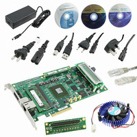
Board, Cables, CD, DVD, Power Supply
Silicon Manufacturer
Altera
Core Architecture
FPGA
Core Sub-architecture
Arria
Silicon Core Number
EP2
Silicon Family Name
Arria II GX
Rohs Compliant
Yes
For Use With/related Products
EP2AGX125EF35
Lead Free Status / RoHS Status
Lead free / RoHS Compliant
Other names
544-2600
Available stocks
Company
Part Number
Manufacturer
Quantity
Price
Company:

Part Number:
DK-DEV-2AGX125N
Manufacturer:
Altera
Quantity:
135


Before You Begin
February 2011 Altera Corporation
Inspect the Board
f
f
1
c
The remaining chapters in this user guide lead you through the following Arria II GX
FPGA development board setup steps:
■
■
■
■
■
For complete information about the FPGA development board, refer to the
FPGA Development Board Reference
Before using the kit or installing the software, check the kit contents and inspect the
board to verify that you received all of the items listed in
If any of the items are missing, contact Altera before you proceed.
To inspect the board, perform the following steps:
1. Place the board on an anti-static surface and inspect it to ensure that it has not been
2. Verify that all components are on the board and appear intact.
In typical applications with the Arria II GX FPGA development board, a heat sink is
not necessary. However, under extreme conditions or for engineering sample silicon
the board might require additional cooling to stay within operating temperature
guidelines. You can perform power consumption and thermal modeling to determine
whether your application requires additional cooling. The board has two holes near
the FPGA that accommodate many different heat sinks, including the Dynatron V31G.
For more information about power consumption and thermal modeling, refer to
AN 358: Thermal Management for
To avoid damage to the board, always have the board POWER switch (SW1) in the
OFF position before inserting the DC power jack (J4).
Inspecting the contents of the kit
Installing the design and kit software
Setting up, powering up, and verifying correct operation of the FPGA
development board
Configuring the Arria II GX FPGA
Running the Board Test System designs
damaged during shipment.
c
Without proper anti-static handling, you can damage the board.
FPGAs.
Manual.
Arria II GX FPGA Development Kit User Guide
2. Getting Started
“Kit Features” on page
Arria II GX
1–1.
Related parts for DK-DEV-2AGX125N
Image
Part Number
Description
Manufacturer
Datasheet
Request
R

Part Number:
Description:
KIT DEV CYCLONE III LS EP3CLS200
Manufacturer:
Altera
Datasheet:

Part Number:
Description:
KIT DEV STRATIX IV FPGA 4SE530
Manufacturer:
Altera
Datasheet:

Part Number:
Description:
KIT DEV FPGA 2AGX260 W/6.375G TX
Manufacturer:
Altera
Datasheet:

Part Number:
Description:
KIT DEV MAX V 5M570Z
Manufacturer:
Altera
Datasheet:

Part Number:
Description:
KIT DEV STRATIX V FPGA 5SGXEA7
Manufacturer:
Altera
Datasheet:

Part Number:
Description:
KIT DEVELOPMENT STRATIX III
Manufacturer:
Altera
Datasheet:

Part Number:
Description:
KIT DEVELOPMENT STRATIX IV
Manufacturer:
Altera
Datasheet:

Part Number:
Description:
KIT DEV ARRIA GX 1AGX60N
Manufacturer:
Altera
Datasheet:
Part Number:
Description:
KIT STARTER CYCLONE IV GX
Manufacturer:
Altera
Datasheet:
Part Number:
Description:
KIT DEVELOPMENT STRATIX IV
Manufacturer:
Altera
Datasheet:

Part Number:
Description:
CPLD, EP610 Family, ECMOS Process, 300 Gates, 16 Macro Cells, 16 Reg., 16 User I/Os, 5V Supply, 35 Speed Grade, 24DIP
Manufacturer:
Altera Corporation
Datasheet:
Part Number:
Description:
CPLD, EP610 Family, ECMOS Process, 300 Gates, 16 Macro Cells, 16 Reg., 16 User I/Os, 5V Supply, 15 Speed Grade, 24DIP
Manufacturer:
Altera Corporation
Datasheet: