DK-DEV-2AGX125N Altera, DK-DEV-2AGX125N Datasheet - Page 37
DK-DEV-2AGX125N
Manufacturer Part Number
DK-DEV-2AGX125N
Description
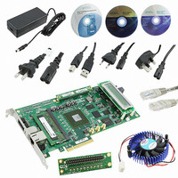
KIT DEV ARRIA II GX FPGA 2AGX125
Manufacturer
Altera
Series
Arria II GXr
Type
FPGAr
Datasheets
1.EP2AGX45CU17C6N.pdf
(96 pages)
2.DK-DEV-2AGX125N.pdf
(48 pages)
3.DK-DEV-2AGX125N.pdf
(64 pages)
Specifications of DK-DEV-2AGX125N
Contents
Board, Cables, CD, DVD, Power Supply
Silicon Manufacturer
Altera
Core Architecture
FPGA
Core Sub-architecture
Arria
Silicon Core Number
EP2
Silicon Family Name
Arria II GX
Rohs Compliant
Yes
For Use With/related Products
EP2AGX125EF35
Lead Free Status / RoHS Status
Lead free / RoHS Compliant
Other names
544-2600
Available stocks
Company
Part Number
Manufacturer
Quantity
Price
Company:

Part Number:
DK-DEV-2AGX125N
Manufacturer:
Altera
Quantity:
135


Chapter 6: Board Test System
Using the Board Test System
February 2011 Altera Corporation
■
■
Error Control
This control displays data errors detected during analysis and allows you to insert
errors:
■
■
■
■
Start
This control initiates HSMC transaction performance analysis.
Stop
This control terminates transaction performance analysis.
Performance Indicators
These controls display current transaction performance analysis information collected
since you last clicked Start:
■
■
Memory—Selects a generic data pattern stored in the on chip memory of the
Arria II GX device.
Math—Selects data generated from a simple math function within the FPGA
fabric.
Detected Errors—Displays the number of data errors detected in the hardware.
Inserted Errors—Displays the number of errors inserted into the transmit data
stream.
Insert Error—Inserts a one-word error into the transmit data stream each time you
click the button. Insert Error is only enabled during transaction performance
analysis.
Clear—Resets the Detected errors and Inserted errors counters to zeros.
TX and RX performance bars—Show the percentage of maximum theoretical data
rate that the requested transactions are able to achieve.
Tx (MBytes/s) and Rx (MBytes/s)—Show the number of bytes of data analyzed
per second. The HSMA transceiver bus is 4 bits wide and the data rate is
3.75 Gbps, totaling 1.5625 GBps full-duplex. The LVDS SERDES bus is 17 bits
wide. The transmit data bus is 16 bits wide and the frequency is 300 MHz double
data rate (600 Mbps per pin), equating to a theoretical maximum bandwidth of
1200 MBps.
Arria II GX FPGA Development Kit User Guide
6–17
Related parts for DK-DEV-2AGX125N
Image
Part Number
Description
Manufacturer
Datasheet
Request
R

Part Number:
Description:
KIT DEV CYCLONE III LS EP3CLS200
Manufacturer:
Altera
Datasheet:

Part Number:
Description:
KIT DEV STRATIX IV FPGA 4SE530
Manufacturer:
Altera
Datasheet:

Part Number:
Description:
KIT DEV FPGA 2AGX260 W/6.375G TX
Manufacturer:
Altera
Datasheet:

Part Number:
Description:
KIT DEV MAX V 5M570Z
Manufacturer:
Altera
Datasheet:

Part Number:
Description:
KIT DEV STRATIX V FPGA 5SGXEA7
Manufacturer:
Altera
Datasheet:

Part Number:
Description:
KIT DEVELOPMENT STRATIX III
Manufacturer:
Altera
Datasheet:

Part Number:
Description:
KIT DEVELOPMENT STRATIX IV
Manufacturer:
Altera
Datasheet:

Part Number:
Description:
KIT DEV ARRIA GX 1AGX60N
Manufacturer:
Altera
Datasheet:
Part Number:
Description:
KIT STARTER CYCLONE IV GX
Manufacturer:
Altera
Datasheet:
Part Number:
Description:
KIT DEVELOPMENT STRATIX IV
Manufacturer:
Altera
Datasheet:

Part Number:
Description:
CPLD, EP610 Family, ECMOS Process, 300 Gates, 16 Macro Cells, 16 Reg., 16 User I/Os, 5V Supply, 35 Speed Grade, 24DIP
Manufacturer:
Altera Corporation
Datasheet:
Part Number:
Description:
CPLD, EP610 Family, ECMOS Process, 300 Gates, 16 Macro Cells, 16 Reg., 16 User I/Os, 5V Supply, 15 Speed Grade, 24DIP
Manufacturer:
Altera Corporation
Datasheet: