DK-DEV-2AGX125N Altera, DK-DEV-2AGX125N Datasheet - Page 30
DK-DEV-2AGX125N
Manufacturer Part Number
DK-DEV-2AGX125N
Description
KIT DEV ARRIA II GX FPGA 2AGX125
Manufacturer
Altera
Series
Arria II GXr
Type
FPGAr
Datasheets
1.EP2AGX45CU17C6N.pdf
(96 pages)
2.DK-DEV-2AGX125N.pdf
(48 pages)
3.DK-DEV-2AGX125N.pdf
(64 pages)
Specifications of DK-DEV-2AGX125N
Contents
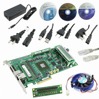
Board, Cables, CD, DVD, Power Supply
Silicon Manufacturer
Altera
Core Architecture
FPGA
Core Sub-architecture
Arria
Silicon Core Number
EP2
Silicon Family Name
Arria II GX
Rohs Compliant
Yes
For Use With/related Products
EP2AGX125EF35
Lead Free Status / RoHS Status
Lead free / RoHS Compliant
Other names
544-2600
Available stocks
Company
Part Number
Manufacturer
Quantity
Price
Company:

Part Number:
DK-DEV-2AGX125N
Manufacturer:
Altera
Quantity:
135


6–10
Figure 6–5. The SSRAM Tab
Arria II GX FPGA Development Kit User Guide
The SSRAM Tab
1
The SSRAM tab allows you to read and write SRAM and flash memory on your
board.
The following sections describe the controls on the SSRAM tab.
Read
This control allows you to read and write the SRAM on your board. Type a starting
address in the text box and click Read. Values starting at the specified address appear
in the table. The base address of SRAM in this Nios II-based BTS design is
0x0D00.0000. The valid address range within the 2-MB SRAM is 0x0000.0000 through
0x001F.FFFF, as shown in the GUI.
If you enter an address outside of the 0x0000.0000 to 0x001F.FFFF SRAM address
space, a warning message identifies the valid SRAM address range.
Figure 6–5
shows the SSRAM tab.
February 2011 Altera Corporation
Chapter 6: Board Test System
Using the Board Test System
Related parts for DK-DEV-2AGX125N
Image
Part Number
Description
Manufacturer
Datasheet
Request
R

Part Number:
Description:
KIT DEV CYCLONE III LS EP3CLS200
Manufacturer:
Altera
Datasheet:

Part Number:
Description:
KIT DEV STRATIX IV FPGA 4SE530
Manufacturer:
Altera
Datasheet:

Part Number:
Description:
KIT DEV FPGA 2AGX260 W/6.375G TX
Manufacturer:
Altera
Datasheet:

Part Number:
Description:
KIT DEV MAX V 5M570Z
Manufacturer:
Altera
Datasheet:

Part Number:
Description:
KIT DEV STRATIX V FPGA 5SGXEA7
Manufacturer:
Altera
Datasheet:

Part Number:
Description:
KIT DEVELOPMENT STRATIX III
Manufacturer:
Altera
Datasheet:

Part Number:
Description:
KIT DEVELOPMENT STRATIX IV
Manufacturer:
Altera
Datasheet:

Part Number:
Description:
KIT DEV ARRIA GX 1AGX60N
Manufacturer:
Altera
Datasheet:
Part Number:
Description:
KIT STARTER CYCLONE IV GX
Manufacturer:
Altera
Datasheet:
Part Number:
Description:
KIT DEVELOPMENT STRATIX IV
Manufacturer:
Altera
Datasheet:

Part Number:
Description:
CPLD, EP610 Family, ECMOS Process, 300 Gates, 16 Macro Cells, 16 Reg., 16 User I/Os, 5V Supply, 35 Speed Grade, 24DIP
Manufacturer:
Altera Corporation
Datasheet:
Part Number:
Description:
CPLD, EP610 Family, ECMOS Process, 300 Gates, 16 Macro Cells, 16 Reg., 16 User I/Os, 5V Supply, 15 Speed Grade, 24DIP
Manufacturer:
Altera Corporation
Datasheet: