DK-DEV-2AGX125N Altera, DK-DEV-2AGX125N Datasheet - Page 40
DK-DEV-2AGX125N
Manufacturer Part Number
DK-DEV-2AGX125N
Description
KIT DEV ARRIA II GX FPGA 2AGX125
Manufacturer
Altera
Series
Arria II GXr
Type
FPGAr
Datasheets
1.EP2AGX45CU17C6N.pdf
(96 pages)
2.DK-DEV-2AGX125N.pdf
(48 pages)
3.DK-DEV-2AGX125N.pdf
(64 pages)
Specifications of DK-DEV-2AGX125N
Contents
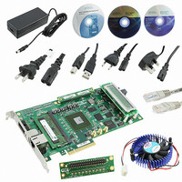
Board, Cables, CD, DVD, Power Supply
Silicon Manufacturer
Altera
Core Architecture
FPGA
Core Sub-architecture
Arria
Silicon Core Number
EP2
Silicon Family Name
Arria II GX
Rohs Compliant
Yes
For Use With/related Products
EP2AGX125EF35
Lead Free Status / RoHS Status
Lead free / RoHS Compliant
Other names
544-2600
Available stocks
Company
Part Number
Manufacturer
Quantity
Price
Company:

Part Number:
DK-DEV-2AGX125N
Manufacturer:
Altera
Quantity:
135


6–20
Configuring the FPGA Using the Quartus II Programmer
Arria II GX FPGA Development Kit User Guide
Calculating Power
1
The Power Monitor calculates power by measuring two different voltages with the
LT2418 A/D and applying the equation P = V × I to determine the power
consumption. The LT2418 measures the voltage after the appropriate sense resistor
(Vsense) and the voltage drop across that sense resistor (Vdif). The current (I) is
calculated by dividing the measured voltage drop across the resistor by the value of
the sense resistor (I = Vdif/R). Through substitution, the equation for calculating
power becomes P = V × I = Vsense × (Vdif/R) = (Vsense) × (Vdif) × (1/.009), except for
the A2VCC rail which uses .001 for R.
You can verify the power numbers shown in the Power Monitor with a digital
multimeter that is capable of measuring microvolts to ensure you have enough
significant digits for an accurate calculation. Measure the voltage on one side of the
resistor (the side opposite the power source) and then measure the voltage on the
other side. The first measurement is Vsense and the difference between the two
measurements is Vdif. Plug the values into the equation to determine the power
consumption.
You can use the Quartus II Programmer to configure the FPGA with a specific .sof.
Before configuring the FPGA, ensure that the Quartus II Programmer and the
USB-Blaster driver are installed on the host computer, the USB cable is connected to
the FPGA development board, power to the board is on, and no other applications
that use the JTAG chain are running.
To configure the Arria II GX FPGA, perform the following steps:
1. Start the Quartus II Programmer.
2. Click Add File and select the path to the desired .sof.
3. Turn on the Program/Configure option for the added file.
4. Click Start to download the selected file to the FPGA. Configuration is complete
Using the Quartus II programmer to configure a device on the board causes other
JTAG-based applications such as the Board Test System and the Power Monitor to
loose their connection to the board. Restart those applications after configuration is
complete.
when the progress bar reaches 100%.
Configuring the FPGA Using the Quartus II Programmer
February 2011 Altera Corporation
Chapter 6: Board Test System
Related parts for DK-DEV-2AGX125N
Image
Part Number
Description
Manufacturer
Datasheet
Request
R

Part Number:
Description:
KIT DEV CYCLONE III LS EP3CLS200
Manufacturer:
Altera
Datasheet:

Part Number:
Description:
KIT DEV STRATIX IV FPGA 4SE530
Manufacturer:
Altera
Datasheet:

Part Number:
Description:
KIT DEV FPGA 2AGX260 W/6.375G TX
Manufacturer:
Altera
Datasheet:

Part Number:
Description:
KIT DEV MAX V 5M570Z
Manufacturer:
Altera
Datasheet:

Part Number:
Description:
KIT DEV STRATIX V FPGA 5SGXEA7
Manufacturer:
Altera
Datasheet:

Part Number:
Description:
KIT DEVELOPMENT STRATIX III
Manufacturer:
Altera
Datasheet:

Part Number:
Description:
KIT DEVELOPMENT STRATIX IV
Manufacturer:
Altera
Datasheet:

Part Number:
Description:
KIT DEV ARRIA GX 1AGX60N
Manufacturer:
Altera
Datasheet:
Part Number:
Description:
KIT STARTER CYCLONE IV GX
Manufacturer:
Altera
Datasheet:
Part Number:
Description:
KIT DEVELOPMENT STRATIX IV
Manufacturer:
Altera
Datasheet:

Part Number:
Description:
CPLD, EP610 Family, ECMOS Process, 300 Gates, 16 Macro Cells, 16 Reg., 16 User I/Os, 5V Supply, 35 Speed Grade, 24DIP
Manufacturer:
Altera Corporation
Datasheet:
Part Number:
Description:
CPLD, EP610 Family, ECMOS Process, 300 Gates, 16 Macro Cells, 16 Reg., 16 User I/Os, 5V Supply, 15 Speed Grade, 24DIP
Manufacturer:
Altera Corporation
Datasheet: