DK-DEV-2AGX125N Altera, DK-DEV-2AGX125N Datasheet - Page 43
DK-DEV-2AGX125N
Manufacturer Part Number
DK-DEV-2AGX125N
Description
KIT DEV ARRIA II GX FPGA 2AGX125
Manufacturer
Altera
Series
Arria II GXr
Type
FPGAr
Datasheets
1.EP2AGX45CU17C6N.pdf
(96 pages)
2.DK-DEV-2AGX125N.pdf
(48 pages)
3.DK-DEV-2AGX125N.pdf
(64 pages)
Specifications of DK-DEV-2AGX125N
Contents
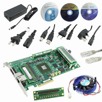
Board, Cables, CD, DVD, Power Supply
Silicon Manufacturer
Altera
Core Architecture
FPGA
Core Sub-architecture
Arria
Silicon Core Number
EP2
Silicon Family Name
Arria II GX
Rohs Compliant
Yes
For Use With/related Products
EP2AGX125EF35
Lead Free Status / RoHS Status
Lead free / RoHS Compliant
Other names
544-2600
Available stocks
Company
Part Number
Manufacturer
Quantity
Price
Company:

Part Number:
DK-DEV-2AGX125N
Manufacturer:
Altera
Quantity:
135


Appendix A
Programming Flash Memory Using the Board Update Portal
sof2flash --input=<yourfile>_hw.sof --output=<yourfile>_hw.flash --offset=0x00640000 --
pfl --optionbit=0x18000 --programmingmode=PSr
elf2flash --base=0x08000000 --end=0x0BFFFFFF --reset=0x0A020000
--input=<yourfile>_sw.elf --output=<yourfile>_sw.flash
--boot=$SOPC_KIT_NIOS2/components/altera_nios2/boot_loader_cfi.srecr
Programming Flash Memory Using the Board Update Portal
Programming Flash Memory Using the Nios II EDS
February 2011 Altera Corporation
1
1
2. In the Nios II command shell, navigate to the directory where your design files
The resulting .flash files are ready for flash device programming. If your design uses
additional files such as image data or files used by the runtime program, you must
first convert the files to .flash format and concatenate them into one .flash file before
using the Board Update Portal to upload them.
The Board Update Portal standard .flash format conventionally uses either
<filename>_hw.flash for hardware design files or <filename>_sw.flash for software
design files.
Once you have the necessary .flash files, you can use the Board Update Portal to
reprogram the flash memory. Refer to
Designs” on page 5–2
If you have generated a .sof that operates without a software design file, you can still
use the Board Update Portal to upload your design. In this case, leave the Software
File Name field blank.
The Nios II EDS offers a nios2-flash-programmer utility to program the flash memory
directly. To program the .flash files or any compatible S-Record File (.srec) to the
board using nios2-flash-programmer, perform the following steps:
1. Set the USER_LOAD switch (SW4.4) to the off position to load the Board Update
2. Attach the USB-Blaster cable and power up the board.
3. If the board has powered up and the LCD displays either "Connecting..." or a valid
4. Launch the Quartus II Programmer to configure the FPGA with a .sof capable of
reside and type the following Nios II EDS commands:
■
■
1
Portal design from flash memory on power up.
IP address (such as 152.198.231.75), proceed to step 8. If no output appears on the
LCD or if the CONF DONE LED (D14) does not illuminate, continue to step
load the FPGA with a flash-writing design.
flash programming. Refer to
Programmer” on page 6–20
For Quartus II .sof files:
For Nios II .elf files:
For boards with dual-die CFI flash devices, use --base=0x0A000000. For
more information, refer to the Board Revision History appendix of the
Arria II GX FPGA Development Board Reference
for more information.
for more information.
“Configuring the FPGA Using the Quartus II
“Using the Board Update Portal to Update User
Arria II GX FPGA Development Kit User Guide
Manual.
4
to
A–3
Related parts for DK-DEV-2AGX125N
Image
Part Number
Description
Manufacturer
Datasheet
Request
R

Part Number:
Description:
KIT DEV CYCLONE III LS EP3CLS200
Manufacturer:
Altera
Datasheet:

Part Number:
Description:
KIT DEV STRATIX IV FPGA 4SE530
Manufacturer:
Altera
Datasheet:

Part Number:
Description:
KIT DEV FPGA 2AGX260 W/6.375G TX
Manufacturer:
Altera
Datasheet:

Part Number:
Description:
KIT DEV MAX V 5M570Z
Manufacturer:
Altera
Datasheet:

Part Number:
Description:
KIT DEV STRATIX V FPGA 5SGXEA7
Manufacturer:
Altera
Datasheet:

Part Number:
Description:
KIT DEVELOPMENT STRATIX III
Manufacturer:
Altera
Datasheet:

Part Number:
Description:
KIT DEVELOPMENT STRATIX IV
Manufacturer:
Altera
Datasheet:

Part Number:
Description:
KIT DEV ARRIA GX 1AGX60N
Manufacturer:
Altera
Datasheet:
Part Number:
Description:
KIT STARTER CYCLONE IV GX
Manufacturer:
Altera
Datasheet:
Part Number:
Description:
KIT DEVELOPMENT STRATIX IV
Manufacturer:
Altera
Datasheet:

Part Number:
Description:
CPLD, EP610 Family, ECMOS Process, 300 Gates, 16 Macro Cells, 16 Reg., 16 User I/Os, 5V Supply, 35 Speed Grade, 24DIP
Manufacturer:
Altera Corporation
Datasheet:
Part Number:
Description:
CPLD, EP610 Family, ECMOS Process, 300 Gates, 16 Macro Cells, 16 Reg., 16 User I/Os, 5V Supply, 15 Speed Grade, 24DIP
Manufacturer:
Altera Corporation
Datasheet: