DK-DEV-2AGX125N Altera, DK-DEV-2AGX125N Datasheet - Page 20
DK-DEV-2AGX125N
Manufacturer Part Number
DK-DEV-2AGX125N
Description
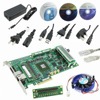
KIT DEV ARRIA II GX FPGA 2AGX125
Manufacturer
Altera
Series
Arria II GXr
Type
FPGAr
Datasheets
1.EP2AGX45CU17C6N.pdf
(96 pages)
2.DK-DEV-2AGX125N.pdf
(48 pages)
3.DK-DEV-2AGX125N.pdf
(64 pages)
Specifications of DK-DEV-2AGX125N
Contents
Board, Cables, CD, DVD, Power Supply
Silicon Manufacturer
Altera
Core Architecture
FPGA
Core Sub-architecture
Arria
Silicon Core Number
EP2
Silicon Family Name
Arria II GX
Rohs Compliant
Yes
For Use With/related Products
EP2AGX125EF35
Lead Free Status / RoHS Status
Lead free / RoHS Compliant
Other names
544-2600
Available stocks
Company
Part Number
Manufacturer
Quantity
Price
Company:

Part Number:
DK-DEV-2AGX125N
Manufacturer:
Altera
Quantity:
135


5–2
Using the Board Update Portal to Update User Designs
Arria II GX FPGA Development Kit User Guide
f
1
1
5. Click Arria II GX FPGA Development Kit on the Board Update Portal web page to
You can also navigate directly to the
Altera website to determine if you have the latest kit software.
The Board Update Portal allows you to write new designs to the user portion of flash
memory. Designs must be in the Nios II Flash Programmer File (.flash) format.
Design files available from the
.flash files. You can also create .flash files from your own custom design. Refer to
“Preparing Design Files for Flash Programming” on page A–2
preparing your own design for upload.
To upload a design over the network into the user portion of flash memory on your
board, perform the following steps:
1. Perform the steps in
2. In the Hardware File Name field specify the .flash file that you either downloaded
3. Click Upload. The progress bar indicates the percent complete.
4. To configure the FPGA with the new design after the flash memory upload process
As long as you don’t overwrite the factory image in the flash memory device, you can
continue to use the Board Update Portal to write new designs to the user portion of
flash memory. If you do overwrite the factory image, you can restore it by following
the instructions in
access the kit’s home page. Visit this page occasionally for documentation updates
and additional new designs.
the Board Update Portal web page.
from the Altera website or created on your own. If there is a software component
to the design, specify it in the same manner using the Software File Name field,
otherwise leave the Software File Name field blank.
is complete, set the USER_LOAD switch (SW4.4) to the on position and power
cycle the board, or press the IMAGE SEL button (PB6) until the CONFIG1 LED
(D12) illuminates and then press the LOAD IMAGE button (PB5). Refer to
Table 6–1 on page 6–5
“Restoring the Flash Device to the Factory Settings” on page
“Connecting to the Board Update Portal Web Page”
for information about the CONFIG LEDs.
Arria II GX FPGA Development Kit
Arria II GX FPGA Development Kit
Using the Board Update Portal to Update User Designs
February 2011 Altera Corporation
Chapter 5: Board Update Portal
for information about
page include
page of the
to access
A–4.
Related parts for DK-DEV-2AGX125N
Image
Part Number
Description
Manufacturer
Datasheet
Request
R

Part Number:
Description:
KIT DEV CYCLONE III LS EP3CLS200
Manufacturer:
Altera
Datasheet:

Part Number:
Description:
KIT DEV STRATIX IV FPGA 4SE530
Manufacturer:
Altera
Datasheet:

Part Number:
Description:
KIT DEV FPGA 2AGX260 W/6.375G TX
Manufacturer:
Altera
Datasheet:

Part Number:
Description:
KIT DEV MAX V 5M570Z
Manufacturer:
Altera
Datasheet:

Part Number:
Description:
KIT DEV STRATIX V FPGA 5SGXEA7
Manufacturer:
Altera
Datasheet:

Part Number:
Description:
KIT DEVELOPMENT STRATIX III
Manufacturer:
Altera
Datasheet:

Part Number:
Description:
KIT DEVELOPMENT STRATIX IV
Manufacturer:
Altera
Datasheet:

Part Number:
Description:
KIT DEV ARRIA GX 1AGX60N
Manufacturer:
Altera
Datasheet:
Part Number:
Description:
KIT STARTER CYCLONE IV GX
Manufacturer:
Altera
Datasheet:
Part Number:
Description:
KIT DEVELOPMENT STRATIX IV
Manufacturer:
Altera
Datasheet:

Part Number:
Description:
CPLD, EP610 Family, ECMOS Process, 300 Gates, 16 Macro Cells, 16 Reg., 16 User I/Os, 5V Supply, 35 Speed Grade, 24DIP
Manufacturer:
Altera Corporation
Datasheet:
Part Number:
Description:
CPLD, EP610 Family, ECMOS Process, 300 Gates, 16 Macro Cells, 16 Reg., 16 User I/Os, 5V Supply, 15 Speed Grade, 24DIP
Manufacturer:
Altera Corporation
Datasheet: