DK-DEV-2AGX125N Altera, DK-DEV-2AGX125N Datasheet - Page 36
DK-DEV-2AGX125N
Manufacturer Part Number
DK-DEV-2AGX125N
Description
KIT DEV ARRIA II GX FPGA 2AGX125
Manufacturer
Altera
Series
Arria II GXr
Type
FPGAr
Datasheets
1.EP2AGX45CU17C6N.pdf
(96 pages)
2.DK-DEV-2AGX125N.pdf
(48 pages)
3.DK-DEV-2AGX125N.pdf
(64 pages)
Specifications of DK-DEV-2AGX125N
Contents
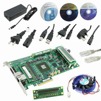
Board, Cables, CD, DVD, Power Supply
Silicon Manufacturer
Altera
Core Architecture
FPGA
Core Sub-architecture
Arria
Silicon Core Number
EP2
Silicon Family Name
Arria II GX
Rohs Compliant
Yes
For Use With/related Products
EP2AGX125EF35
Lead Free Status / RoHS Status
Lead free / RoHS Compliant
Other names
544-2600
Available stocks
Company
Part Number
Manufacturer
Quantity
Price
Company:

Part Number:
DK-DEV-2AGX125N
Manufacturer:
Altera
Quantity:
135


6–16
Arria II GX FPGA Development Kit User Guide
f
1
You must have the loopback HSMC installed on the HSMC connector that you are
testing for this test to work correctly.
The following sections describe the controls on the HSMC tab.
Status
This control displays the following status information during the loopback test:
■
■
■
Port
This control allows you to specify the type of test to run on the HSMC ports. The
following HSMC port tests are available:
■
■
■
PMA Setting
The PMA Setting button allows you to make changes to the PMA parameters that
affect the active transceiver interface. The following settings are available for analysis:
■
■
■
■
■
For restrictions on the PMA settings, refer to
Device Handbook.
Data Type
This control specifies the type of data contained in the transactions. The following
data types are available for analysis:
■
PLL lock—Shows the PLL locked or unlocked state.
Channel lock—Shows the channel locked or unlocked state. When locked, all
lanes are word aligned and channel bonded.
Pattern sync—Shows the pattern synced or not synced state. The pattern is
considered synced when the start of the data sequence is detected.
HSMA x4 Tranceivers [0..3]
HSMA x17 LVDS SERDES
HSMA x3 single-ended loopback
Serial Loopback—Routes signals from the receiver to the transmitter.
VOD—Specifies the voltage output differential of the transmitter buffer.
Pre-emphasis tap
■
■
■
Equalizer—Specifies the setting for the receiver equalizer.
DC gain—Specifies the DC portion of the receiver equalizer.
PRBS—Selects pseudo-random bit sequences.
Pre—Specifies the amount of pre-emphasis on the pre-tap of the transmitter
buffer.
First post—Specifies the amount of pre-emphasis on the first post tap of the
transmitter buffer.
Second post—Specifies the amount of pre-emphasis on the second post tap of
the transmitter buffer.
Volume 2: Transceivers
February 2011 Altera Corporation
Chapter 6: Board Test System
Using the Board Test System
of the Arria II
Related parts for DK-DEV-2AGX125N
Image
Part Number
Description
Manufacturer
Datasheet
Request
R

Part Number:
Description:
KIT DEV CYCLONE III LS EP3CLS200
Manufacturer:
Altera
Datasheet:

Part Number:
Description:
KIT DEV STRATIX IV FPGA 4SE530
Manufacturer:
Altera
Datasheet:

Part Number:
Description:
KIT DEV FPGA 2AGX260 W/6.375G TX
Manufacturer:
Altera
Datasheet:

Part Number:
Description:
KIT DEV MAX V 5M570Z
Manufacturer:
Altera
Datasheet:

Part Number:
Description:
KIT DEV STRATIX V FPGA 5SGXEA7
Manufacturer:
Altera
Datasheet:

Part Number:
Description:
KIT DEVELOPMENT STRATIX III
Manufacturer:
Altera
Datasheet:

Part Number:
Description:
KIT DEVELOPMENT STRATIX IV
Manufacturer:
Altera
Datasheet:

Part Number:
Description:
KIT DEV ARRIA GX 1AGX60N
Manufacturer:
Altera
Datasheet:
Part Number:
Description:
KIT STARTER CYCLONE IV GX
Manufacturer:
Altera
Datasheet:
Part Number:
Description:
KIT DEVELOPMENT STRATIX IV
Manufacturer:
Altera
Datasheet:

Part Number:
Description:
CPLD, EP610 Family, ECMOS Process, 300 Gates, 16 Macro Cells, 16 Reg., 16 User I/Os, 5V Supply, 35 Speed Grade, 24DIP
Manufacturer:
Altera Corporation
Datasheet:
Part Number:
Description:
CPLD, EP610 Family, ECMOS Process, 300 Gates, 16 Macro Cells, 16 Reg., 16 User I/Os, 5V Supply, 15 Speed Grade, 24DIP
Manufacturer:
Altera Corporation
Datasheet: