C8051T630DK Silicon Laboratories Inc, C8051T630DK Datasheet - Page 74
C8051T630DK
Manufacturer Part Number
C8051T630DK
Description
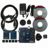
KIT DEV FOR C8051T630 FAMILY
Manufacturer
Silicon Laboratories Inc
Type
MCUr
Specifications of C8051T630DK
Contents
Board, daughter boards, power adapter, cables, documentation and software
Processor To Be Evaluated
C8051T63x
Interface Type
USB
Lead Free Status / RoHS Status
Lead free / RoHS Compliant
For Use With/related Products
C8051T630, T631, T632, T633, T634 and T635 MCUs
For Use With
336-1465 - BOARD SOCKET DAUGHTER 20-QFN
Lead Free Status / Rohs Status
Lead free / RoHS Compliant
Other names
336-1464


C8051T630/1/2/3/4/5
13.2.1.1. General Purpose Registers
The lower 32 bytes of data memory, locations 0x00 through 0x1F, may be addressed as four banks of gen-
eral-purpose registers. Each bank consists of eight byte-wide registers designated R0 through R7. Only
one of these banks may be enabled at a time. Two bits in the program status word, RS0 (PSW.3) and RS1
(PSW.4), select the active register bank (see description of the PSW in SFR Definition 12.6). This allows
fast context switching when entering subroutines and interrupt service routines. Indirect addressing modes
use registers R0 and R1 as index registers.
13.2.1.2. Bit Addressable Locations
In addition to direct access to data memory organized as bytes, the sixteen data memory locations at 0x20
through 0x2F are also accessible as 128 individually addressable bits. Each bit has a bit address from
0x00 to 0x7F. Bit 0 of the byte at 0x20 has bit address 0x00 while bit7 of the byte at 0x20 has bit address
0x07. Bit 7 of the byte at 0x2F has bit address 0x7F. A bit access is distinguished from a full byte access by
the type of instruction used (bit source or destination operands as opposed to a byte source or destina-
tion).
The MCS-51™ assembly language allows an alternate notation for bit addressing of the form XX.B where
XX is the byte address and B is the bit position within the byte. For example, the instruction:
MOV
C, 22.3h
moves the Boolean value at 0x13 (bit 3 of the byte at location 0x22) into the Carry flag.
13.2.1.3. Stack
A programmer's stack can be located anywhere in the 256-byte data memory. The stack area is desig-
nated using the Stack Pointer (SP) SFR. The SP will point to the last location used. The next value pushed
on the stack is placed at SP+1 and then SP is incremented. A reset initializes the stack pointer to location
0x07. Therefore, the first value pushed on the stack is placed at location 0x08, which is also the first regis-
ter (R0) of register bank 1. Thus, if more than one register bank is to be used, the SP should be initialized
to a location in the data memory not being used for data storage. The stack depth can extend up to
256 bytes.
13.2.2. External RAM
There are 512 bytes of on-chip RAM mapped into the external data memory space. All of these address
locations may be accessed using the external move instruction (MOVX) and the data pointer (DPTR), or
using MOVX indirect addressing mode. If the MOVX instruction is used with an 8-bit address operand
(such as @R1), then the high byte of the 16-bit address is provided by the External Memory Interface Con-
trol Register (EMI0CN as shown in SFR Definition 13.1).
For a 16-bit MOVX operation (@DPTR), the upper 7 bits of the 16-bit external data memory address word
are "don't cares". As a result, the 512-byte RAM is mapped modulo style over the entire 64 k external data
memory address range. For example, the XRAM byte at address 0x0000 is shadowed at addresses
0x0200, 0x0400, 0x0600, 0x0800, etc. This is a useful feature when performing a linear memory fill, as the
address pointer doesn't have to be reset when reaching the RAM block boundary.
74
Rev. 1.0
Related parts for C8051T630DK
Image
Part Number
Description
Manufacturer
Datasheet
Request
R

Part Number:
Description:
SMD/C°/SINGLE-ENDED OUTPUT SILICON OSCILLATOR
Manufacturer:
Silicon Laboratories Inc
Part Number:
Description:
Manufacturer:
Silicon Laboratories Inc
Datasheet:
Part Number:
Description:
N/A N/A/SI4010 AES KEYFOB DEMO WITH LCD RX
Manufacturer:
Silicon Laboratories Inc
Datasheet:
Part Number:
Description:
N/A N/A/SI4010 SIMPLIFIED KEY FOB DEMO WITH LED RX
Manufacturer:
Silicon Laboratories Inc
Datasheet:
Part Number:
Description:
N/A/-40 TO 85 OC/EZLINK MODULE; F930/4432 HIGH BAND (REV E/B1)
Manufacturer:
Silicon Laboratories Inc
Part Number:
Description:
EZLink Module; F930/4432 Low Band (rev e/B1)
Manufacturer:
Silicon Laboratories Inc
Part Number:
Description:
I°/4460 10 DBM RADIO TEST CARD 434 MHZ
Manufacturer:
Silicon Laboratories Inc
Part Number:
Description:
I°/4461 14 DBM RADIO TEST CARD 868 MHZ
Manufacturer:
Silicon Laboratories Inc
Part Number:
Description:
I°/4463 20 DBM RFSWITCH RADIO TEST CARD 460 MHZ
Manufacturer:
Silicon Laboratories Inc
Part Number:
Description:
I°/4463 20 DBM RADIO TEST CARD 868 MHZ
Manufacturer:
Silicon Laboratories Inc
Part Number:
Description:
I°/4463 27 DBM RADIO TEST CARD 868 MHZ
Manufacturer:
Silicon Laboratories Inc
Part Number:
Description:
I°/4463 SKYWORKS 30 DBM RADIO TEST CARD 915 MHZ
Manufacturer:
Silicon Laboratories Inc
Part Number:
Description:
N/A N/A/-40 TO 85 OC/4463 RFMD 30 DBM RADIO TEST CARD 915 MHZ
Manufacturer:
Silicon Laboratories Inc
Part Number:
Description:
I°/4463 20 DBM RADIO TEST CARD 169 MHZ
Manufacturer:
Silicon Laboratories Inc