C8051T630DK Silicon Laboratories Inc, C8051T630DK Datasheet - Page 5
C8051T630DK
Manufacturer Part Number
C8051T630DK
Description
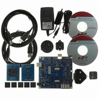
KIT DEV FOR C8051T630 FAMILY
Manufacturer
Silicon Laboratories Inc
Type
MCUr
Specifications of C8051T630DK
Contents
Board, daughter boards, power adapter, cables, documentation and software
Processor To Be Evaluated
C8051T63x
Interface Type
USB
Lead Free Status / RoHS Status
Lead free / RoHS Compliant
For Use With/related Products
C8051T630, T631, T632, T633, T634 and T635 MCUs
For Use With
336-1465 - BOARD SOCKET DAUGHTER 20-QFN
Lead Free Status / Rohs Status
Lead free / RoHS Compliant
Other names
336-1464


21. SMBus................................................................................................................... 127
22. UART0 ................................................................................................................... 148
23. Enhanced Serial Peripheral Interface (SPI0) ..................................................... 156
24. Timers ................................................................................................................... 169
20.3. Priority Crossbar Decoder ............................................................................. 114
20.4. Port I/O Initialization ...................................................................................... 116
20.5. Port Match ..................................................................................................... 118
20.6. Special Function Registers for Accessing and Configuring Port I/O ............. 121
21.1. Supporting Documents .................................................................................. 128
21.2. SMBus Configuration..................................................................................... 128
21.3. SMBus Operation .......................................................................................... 128
21.4. Using the SMBus........................................................................................... 130
21.5. SMBus Transfer Modes................................................................................. 140
21.6. SMBus Status Decoding................................................................................ 143
22.1. Enhanced Baud Rate Generation.................................................................. 149
22.2. Operational Modes ........................................................................................ 150
22.3. Multiprocessor Communications ................................................................... 152
23.1. Signal Descriptions........................................................................................ 157
23.2. SPI0 Master Mode Operation ........................................................................ 158
23.3. SPI0 Slave Mode Operation .......................................................................... 159
23.4. SPI0 Interrupt Sources .................................................................................. 160
23.5. Serial Clock Phase and Polarity .................................................................... 160
23.6. SPI Special Function Registers ..................................................................... 162
24.1. Timer 0 and Timer 1 ...................................................................................... 171
21.3.1. Transmitter Vs. Receiver....................................................................... 129
21.3.2. Arbitration.............................................................................................. 129
21.3.3. Clock Low Extension............................................................................. 129
21.3.4. SCL Low Timeout.................................................................................. 129
21.3.5. SCL High (SMBus Free) Timeout ......................................................... 130
21.4.1. SMBus Configuration Register.............................................................. 130
21.4.2. SMB0CN Control Register .................................................................... 134
21.4.3. Hardware Slave Address Recognition .................................................. 136
21.4.4. Data Register ........................................................................................ 139
21.5.1. Write Sequence (Master) ...................................................................... 140
21.5.2. Read Sequence (Master) ...................................................................... 141
21.5.3. Write Sequence (Slave) ........................................................................ 142
21.5.4. Read Sequence (Slave) ........................................................................ 143
22.2.1. 8-Bit UART ............................................................................................ 150
22.2.2. 9-Bit UART ............................................................................................ 151
23.1.1. Master Out, Slave In (MOSI)................................................................. 157
23.1.2. Master In, Slave Out (MISO)................................................................. 157
23.1.3. Serial Clock (SCK) ................................................................................ 157
23.1.4. Slave Select (NSS) ............................................................................... 157
21.4.2.1. Software ACK Generation ............................................................ 134
21.4.2.2. Hardware ACK Generation ........................................................... 134
Rev. 1.0
C8051T630/1/2/3/4/5
5
Related parts for C8051T630DK
Image
Part Number
Description
Manufacturer
Datasheet
Request
R

Part Number:
Description:
SMD/C°/SINGLE-ENDED OUTPUT SILICON OSCILLATOR
Manufacturer:
Silicon Laboratories Inc
Part Number:
Description:
Manufacturer:
Silicon Laboratories Inc
Datasheet:
Part Number:
Description:
N/A N/A/SI4010 AES KEYFOB DEMO WITH LCD RX
Manufacturer:
Silicon Laboratories Inc
Datasheet:
Part Number:
Description:
N/A N/A/SI4010 SIMPLIFIED KEY FOB DEMO WITH LED RX
Manufacturer:
Silicon Laboratories Inc
Datasheet:
Part Number:
Description:
N/A/-40 TO 85 OC/EZLINK MODULE; F930/4432 HIGH BAND (REV E/B1)
Manufacturer:
Silicon Laboratories Inc
Part Number:
Description:
EZLink Module; F930/4432 Low Band (rev e/B1)
Manufacturer:
Silicon Laboratories Inc
Part Number:
Description:
I°/4460 10 DBM RADIO TEST CARD 434 MHZ
Manufacturer:
Silicon Laboratories Inc
Part Number:
Description:
I°/4461 14 DBM RADIO TEST CARD 868 MHZ
Manufacturer:
Silicon Laboratories Inc
Part Number:
Description:
I°/4463 20 DBM RFSWITCH RADIO TEST CARD 460 MHZ
Manufacturer:
Silicon Laboratories Inc
Part Number:
Description:
I°/4463 20 DBM RADIO TEST CARD 868 MHZ
Manufacturer:
Silicon Laboratories Inc
Part Number:
Description:
I°/4463 27 DBM RADIO TEST CARD 868 MHZ
Manufacturer:
Silicon Laboratories Inc
Part Number:
Description:
I°/4463 SKYWORKS 30 DBM RADIO TEST CARD 915 MHZ
Manufacturer:
Silicon Laboratories Inc
Part Number:
Description:
N/A N/A/-40 TO 85 OC/4463 RFMD 30 DBM RADIO TEST CARD 915 MHZ
Manufacturer:
Silicon Laboratories Inc
Part Number:
Description:
I°/4463 20 DBM RADIO TEST CARD 169 MHZ
Manufacturer:
Silicon Laboratories Inc