C8051T630DK Silicon Laboratories Inc, C8051T630DK Datasheet - Page 24
C8051T630DK
Manufacturer Part Number
C8051T630DK
Description
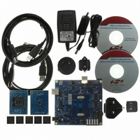
KIT DEV FOR C8051T630 FAMILY
Manufacturer
Silicon Laboratories Inc
Type
MCUr
Specifications of C8051T630DK
Contents
Board, daughter boards, power adapter, cables, documentation and software
Processor To Be Evaluated
C8051T63x
Interface Type
USB
Lead Free Status / RoHS Status
Lead free / RoHS Compliant
For Use With/related Products
C8051T630, T631, T632, T633, T634 and T635 MCUs
For Use With
336-1465 - BOARD SOCKET DAUGHTER 20-QFN
Lead Free Status / Rohs Status
Lead free / RoHS Compliant
Other names
336-1464


C8051T630/1/2/3/4/5
5.2. Electrical Characteristics
Table 5.2. Global Electrical Characteristics
–40 to +85 °C, 25 MHz system clock unless otherwise specified.
24
Parameter
Supply Voltage (Note 1)
Digital Supply Current with
CPU Active
Digital Supply Current with
CPU Inactive (not accessing
EPROM)
Digital Supply Current
(shutdown)
Digital Supply RAM Data
Retention Voltage
Specified Operating Tempera-
ture Range
SYSCLK (system clock
frequency)
Tsysl (SYSCLK low time)
Tsysh (SYSCLK high time)
Notes:
1. Analog performance is not guaranteed when V
2. SYSCLK must be at least 32 kHz to enable debugging.
Regulator in Normal Mode
Regulator in Bypass Mode
V
V
V
V
V
V
V
V
Oscillator not running (stop mode),
Internal Regulator Off
Oscillator not running (stop or sus-
pend mode), Internal Regulator On
(Note 2)
DD
DD
DD
DD
DD
DD
DD
DD
= 1.8 V, Clock = 25 MHz
= 1.8 V, Clock = 1 MHz
= 3.0 V, Clock = 25 MHz
= 3.0 V, Clock = 1 MHz
= 1.8 V, Clock = 25 MHz
= 1.8 V, Clock = 1 MHz
= 3.0 V, Clock = 25 MHz
= 3.0 V, Clock = 1 MHz
Conditions
DD
Rev. 1.0
is below 1.8 V.
Min
–40
1.8
1.7
18
18
—
—
—
—
—
—
—
—
—
—
—
0
0.41
0.42
Typ
350
3.0
1.8
6.2
2.7
2.9
2.2
2.3
0.2
1.5
—
—
—
—
7
Max
+85
400
3.6
1.9
8.8
8.9
3.1
25
—
—
—
—
—
—
—
3
2
Units
MHz
mA
mA
mA
mA
mA
mA
mA
mA
µA
µA
°C
ns
ns
V
V
V
Related parts for C8051T630DK
Image
Part Number
Description
Manufacturer
Datasheet
Request
R

Part Number:
Description:
SMD/C°/SINGLE-ENDED OUTPUT SILICON OSCILLATOR
Manufacturer:
Silicon Laboratories Inc
Part Number:
Description:
Manufacturer:
Silicon Laboratories Inc
Datasheet:
Part Number:
Description:
N/A N/A/SI4010 AES KEYFOB DEMO WITH LCD RX
Manufacturer:
Silicon Laboratories Inc
Datasheet:
Part Number:
Description:
N/A N/A/SI4010 SIMPLIFIED KEY FOB DEMO WITH LED RX
Manufacturer:
Silicon Laboratories Inc
Datasheet:
Part Number:
Description:
N/A/-40 TO 85 OC/EZLINK MODULE; F930/4432 HIGH BAND (REV E/B1)
Manufacturer:
Silicon Laboratories Inc
Part Number:
Description:
EZLink Module; F930/4432 Low Band (rev e/B1)
Manufacturer:
Silicon Laboratories Inc
Part Number:
Description:
I°/4460 10 DBM RADIO TEST CARD 434 MHZ
Manufacturer:
Silicon Laboratories Inc
Part Number:
Description:
I°/4461 14 DBM RADIO TEST CARD 868 MHZ
Manufacturer:
Silicon Laboratories Inc
Part Number:
Description:
I°/4463 20 DBM RFSWITCH RADIO TEST CARD 460 MHZ
Manufacturer:
Silicon Laboratories Inc
Part Number:
Description:
I°/4463 20 DBM RADIO TEST CARD 868 MHZ
Manufacturer:
Silicon Laboratories Inc
Part Number:
Description:
I°/4463 27 DBM RADIO TEST CARD 868 MHZ
Manufacturer:
Silicon Laboratories Inc
Part Number:
Description:
I°/4463 SKYWORKS 30 DBM RADIO TEST CARD 915 MHZ
Manufacturer:
Silicon Laboratories Inc
Part Number:
Description:
N/A N/A/-40 TO 85 OC/4463 RFMD 30 DBM RADIO TEST CARD 915 MHZ
Manufacturer:
Silicon Laboratories Inc
Part Number:
Description:
I°/4463 20 DBM RADIO TEST CARD 169 MHZ
Manufacturer:
Silicon Laboratories Inc