C8051T630DK Silicon Laboratories Inc, C8051T630DK Datasheet - Page 3
C8051T630DK
Manufacturer Part Number
C8051T630DK
Description
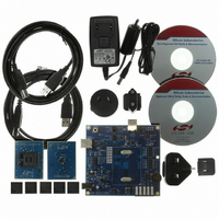
KIT DEV FOR C8051T630 FAMILY
Manufacturer
Silicon Laboratories Inc
Type
MCUr
Specifications of C8051T630DK
Contents
Board, daughter boards, power adapter, cables, documentation and software
Processor To Be Evaluated
C8051T63x
Interface Type
USB
Lead Free Status / RoHS Status
Lead free / RoHS Compliant
For Use With/related Products
C8051T630, T631, T632, T633, T634 and T635 MCUs
For Use With
336-1465 - BOARD SOCKET DAUGHTER 20-QFN
Lead Free Status / Rohs Status
Lead free / RoHS Compliant
Other names
336-1464


Table of Contents
1. System Overview ..................................................................................................... 15
2. Ordering Information ............................................................................................... 17
3. Pin Definitions.......................................................................................................... 18
4. QFN-20 Package Specifications ............................................................................. 21
5. Electrical Characteristics ........................................................................................ 23
6. 10-Bit ADC (ADC0, C8051T630/2/4 only)................................................................ 33
7. Temperature Sensor (C8051T630/2/4 only) ........................................................... 45
8. 10-Bit Current Mode DAC (IDA0, C8051T630/2/4 only) ......................................... 48
9. Voltage Reference Options ..................................................................................... 52
10. Voltage Regulator (REG0) ..................................................................................... 55
11. Comparator0........................................................................................................... 57
12. CIP-51 Microcontroller........................................................................................... 63
13. Memory Organization ............................................................................................ 72
14. Special Function Registers................................................................................... 76
5.1. Absolute Maximum Specifications..................................................................... 23
5.2. Electrical Characteristics ................................................................................... 24
5.3. Typical Performance Curves ............................................................................. 32
6.1. Output Code Formatting .................................................................................... 34
6.2. 8-Bit Mode ......................................................................................................... 34
6.3. Modes of Operation ........................................................................................... 34
6.4. Programmable Window Detector....................................................................... 40
6.5. ADC0 Analog Multiplexer (C8051T630/2/4 only)............................................... 43
7.1. Calibration ......................................................................................................... 45
8.1. IDA0 Output Scheduling .................................................................................... 48
8.2. IDAC Output Mapping ....................................................................................... 49
11.1. Comparator Multiplexer ................................................................................... 61
12.1. Instruction Set.................................................................................................. 64
12.2. CIP-51 Register Descriptions .......................................................................... 69
13.1. Program Memory............................................................................................. 73
13.2. Data Memory ................................................................................................... 73
6.3.1. Starting a Conversion................................................................................ 34
6.3.2. Tracking Modes......................................................................................... 35
6.3.3. Settling Time Requirements...................................................................... 36
6.4.1. Window Detector Example........................................................................ 42
8.1.1. Update Output On-Demand ...................................................................... 48
8.1.2. Update Output Based on Timer Overflow ................................................. 49
8.1.3. Update Output Based on CNVSTR Edge ................................................. 49
12.1.1. Instruction and CPU Timing .................................................................... 64
13.2.1. Internal RAM ........................................................................................... 73
13.2.2. External RAM .......................................................................................... 74
13.2.1.1. General Purpose Registers ............................................................ 74
13.2.1.2. Bit Addressable Locations .............................................................. 74
13.2.1.3. Stack ............................................................................................ 74
Rev. 1.0
C8051T630/1/2/3/4/5
3
Related parts for C8051T630DK
Image
Part Number
Description
Manufacturer
Datasheet
Request
R

Part Number:
Description:
SMD/C°/SINGLE-ENDED OUTPUT SILICON OSCILLATOR
Manufacturer:
Silicon Laboratories Inc
Part Number:
Description:
Manufacturer:
Silicon Laboratories Inc
Datasheet:
Part Number:
Description:
N/A N/A/SI4010 AES KEYFOB DEMO WITH LCD RX
Manufacturer:
Silicon Laboratories Inc
Datasheet:
Part Number:
Description:
N/A N/A/SI4010 SIMPLIFIED KEY FOB DEMO WITH LED RX
Manufacturer:
Silicon Laboratories Inc
Datasheet:
Part Number:
Description:
N/A/-40 TO 85 OC/EZLINK MODULE; F930/4432 HIGH BAND (REV E/B1)
Manufacturer:
Silicon Laboratories Inc
Part Number:
Description:
EZLink Module; F930/4432 Low Band (rev e/B1)
Manufacturer:
Silicon Laboratories Inc
Part Number:
Description:
I°/4460 10 DBM RADIO TEST CARD 434 MHZ
Manufacturer:
Silicon Laboratories Inc
Part Number:
Description:
I°/4461 14 DBM RADIO TEST CARD 868 MHZ
Manufacturer:
Silicon Laboratories Inc
Part Number:
Description:
I°/4463 20 DBM RFSWITCH RADIO TEST CARD 460 MHZ
Manufacturer:
Silicon Laboratories Inc
Part Number:
Description:
I°/4463 20 DBM RADIO TEST CARD 868 MHZ
Manufacturer:
Silicon Laboratories Inc
Part Number:
Description:
I°/4463 27 DBM RADIO TEST CARD 868 MHZ
Manufacturer:
Silicon Laboratories Inc
Part Number:
Description:
I°/4463 SKYWORKS 30 DBM RADIO TEST CARD 915 MHZ
Manufacturer:
Silicon Laboratories Inc
Part Number:
Description:
N/A N/A/-40 TO 85 OC/4463 RFMD 30 DBM RADIO TEST CARD 915 MHZ
Manufacturer:
Silicon Laboratories Inc
Part Number:
Description:
I°/4463 20 DBM RADIO TEST CARD 169 MHZ
Manufacturer:
Silicon Laboratories Inc