C8051T630DK Silicon Laboratories Inc, C8051T630DK Datasheet - Page 56
C8051T630DK
Manufacturer Part Number
C8051T630DK
Description
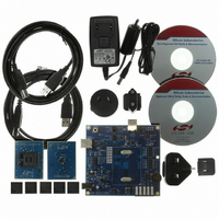
KIT DEV FOR C8051T630 FAMILY
Manufacturer
Silicon Laboratories Inc
Type
MCUr
Specifications of C8051T630DK
Contents
Board, daughter boards, power adapter, cables, documentation and software
Processor To Be Evaluated
C8051T63x
Interface Type
USB
Lead Free Status / RoHS Status
Lead free / RoHS Compliant
For Use With/related Products
C8051T630, T631, T632, T633, T634 and T635 MCUs
For Use With
336-1465 - BOARD SOCKET DAUGHTER 20-QFN
Lead Free Status / Rohs Status
Lead free / RoHS Compliant
Other names
336-1464


C8051T630/1/2/3/4/5
SFR Definition 10.1. REG0CN: Voltage Regulator Control
SFR Address = 0xC7
56
Name
Reset
5:1
Bit
Type
7
6
0
Bit
Reserved Reserved. Must Write 00000b
STOPCF Stop Mode Configuration.
BYPASS Bypass Internal Regulator.
MPCE
Name
STOPCF
R/W
7
0
This bit configures the regulator’s behavior when the device enters STOP mode.
0: Regulator is still active in STOP mode. Any enabled reset source will reset the
device.
1: Regulator is shut down in STOP mode. Only the RST pin or power cycle can reset
the device.
This bit places the regulator in bypass mode, turning off the regulator, and allowing the
core to run directly from the V
0: Normal Mode—Regulator is on.
1: Bypass Mode—Regulator is off, and the microcontroller core operates directly from
the V
IMPORTANT: Bypass mode is for use with an external regulator as the supply
voltage only. Never place the regulator in bypass mode when the V
voltage is greater than the specifications given in Table 5.1 on page 23. Doing so
may cause permanent damage to the device.
Memory Power Controller Enable.
This bit can help the system save power at slower system clock frequencies (about
2.0 MHz or less) by automatically shutting down the EPROM memory between clocks
when information is not being fetched from the EPROM memory.
0: Normal Mode—Memory power controller disabled (EPROM memory is always on).
1: Low Power Mode—Memory power controller enabled (EPROM memory turns on/off
as needed).
Note: If an external clock source is used with the Memory Power Controller enabled, and the
BYPASS
DD
R/W
clock frequency changes from slow (<2.0 MHz) to fast (> 2.0 MHz), the EPROM power
will turn on, and up to 20 clocks may be "skipped" to ensure that the EPROM power is
stable before reading memory.
6
0
supply voltage.
R/W
5
0
DD
R/W
Rev. 1.0
4
0
supply pin.
Function
R/W
3
0
R/W
2
0
R/W
1
0
DD
supply
MPCE
R/W
0
0
Related parts for C8051T630DK
Image
Part Number
Description
Manufacturer
Datasheet
Request
R

Part Number:
Description:
SMD/C°/SINGLE-ENDED OUTPUT SILICON OSCILLATOR
Manufacturer:
Silicon Laboratories Inc
Part Number:
Description:
Manufacturer:
Silicon Laboratories Inc
Datasheet:
Part Number:
Description:
N/A N/A/SI4010 AES KEYFOB DEMO WITH LCD RX
Manufacturer:
Silicon Laboratories Inc
Datasheet:
Part Number:
Description:
N/A N/A/SI4010 SIMPLIFIED KEY FOB DEMO WITH LED RX
Manufacturer:
Silicon Laboratories Inc
Datasheet:
Part Number:
Description:
N/A/-40 TO 85 OC/EZLINK MODULE; F930/4432 HIGH BAND (REV E/B1)
Manufacturer:
Silicon Laboratories Inc
Part Number:
Description:
EZLink Module; F930/4432 Low Band (rev e/B1)
Manufacturer:
Silicon Laboratories Inc
Part Number:
Description:
I°/4460 10 DBM RADIO TEST CARD 434 MHZ
Manufacturer:
Silicon Laboratories Inc
Part Number:
Description:
I°/4461 14 DBM RADIO TEST CARD 868 MHZ
Manufacturer:
Silicon Laboratories Inc
Part Number:
Description:
I°/4463 20 DBM RFSWITCH RADIO TEST CARD 460 MHZ
Manufacturer:
Silicon Laboratories Inc
Part Number:
Description:
I°/4463 20 DBM RADIO TEST CARD 868 MHZ
Manufacturer:
Silicon Laboratories Inc
Part Number:
Description:
I°/4463 27 DBM RADIO TEST CARD 868 MHZ
Manufacturer:
Silicon Laboratories Inc
Part Number:
Description:
I°/4463 SKYWORKS 30 DBM RADIO TEST CARD 915 MHZ
Manufacturer:
Silicon Laboratories Inc
Part Number:
Description:
N/A N/A/-40 TO 85 OC/4463 RFMD 30 DBM RADIO TEST CARD 915 MHZ
Manufacturer:
Silicon Laboratories Inc
Part Number:
Description:
I°/4463 20 DBM RADIO TEST CARD 169 MHZ
Manufacturer:
Silicon Laboratories Inc