STEVAL-ISB005V1 STMicroelectronics, STEVAL-ISB005V1 Datasheet - Page 60
STEVAL-ISB005V1
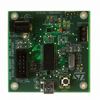
Manufacturer Part Number
STEVAL-ISB005V1
Description
BOARD EVAL CHARGER ST7260/L6924D
Manufacturer
STMicroelectronics
Type
Battery Managementr
Specifications of STEVAL-ISB005V1
Main Purpose
Power Management, Battery Charger
Embedded
Yes, MCU, 8-Bit
Utilized Ic / Part
L6924, ST72F63BK6M1
Primary Attributes
1 Cell- Li-Ion / Li-Pol, 5 V (USB Input)
Secondary Attributes
Powered by Wall Adaptor Also, LED Status Indicators
Input Voltage
5 V
Product
Power Management Modules
Lead Free Status / RoHS Status
Lead free / RoHS Compliant
For Use With/related Products
L6924D, ST7260
Other names
497-8428
Available stocks
Company
Part Number
Manufacturer
Quantity
Price
Company:

Part Number:
STEVAL-ISB005V1
Manufacturer:
STMicroelectronics
Quantity:
1


Watchdog timer (WDG)
60/139
Figure 36. Pulse width modulation mode timing example with two output compare
1. OC1R = 2ED0h, OC2R = 34E2, OLVL1 = 0, OLVL2 = 1
2. On timers with only one Output Compare register, a fixed frequency PWM signal can be generated using
Pulse width modulation mode
Pulse Width Modulation (PWM) mode enables the generation of a signal with a frequency
and pulse length determined by the value of the OC1R and OC2R registers.
Pulse Width Modulation mode uses the complete Output Compare 1 function plus the
OC2R register, and so this functionality can not be used when PWM mode is activated.
In PWM mode, double buffering is implemented on the output compare registers. Any new
values written in the OC1R and OC2R registers are taken into account only at the end of the
PWM period (OC2) to avoid spikes on the PWM output pin (OCMP1).
Procedure
To use Pulse Width Modulation mode:
1.
2.
3.
4.
the output compare and the counter overflow to define the pulse length.
Load the OC2R register with the value corresponding to the period of the signal using
the formula below.
Load the OC1R register with the value corresponding to the period of the pulse if
(OLVL1 = 0 and OLVL2 = 1) using the formula in the opposite column.
Select the following in the CR1 register:
–
–
Select the following in the CR2 register:
–
–
–
Using the OLVL1 bit, select the level to be applied to the OCMP1 pin after a
successful comparison with the OC1R register.
Using the OLVL2 bit, select the level to be applied to the OCMP1 pin after a
successful comparison with the OC2R register.
Set OC1E bit: the OCMP1 pin is then dedicated to the output compare 1 function.
Set the PWM bit.
Select the timer clock (CC[1:0]) (see
functions
Counter 34E2
OCMP1
compare2
(1)(2)
FFFC FFFD FFFE
OLVL2
Table
compare1
2ED0 2ED1 2ED2
32).
OLVL1
compare2
34E2
OLVL2
FFFC
ST7260xx
Related parts for STEVAL-ISB005V1
Image
Part Number
Description
Manufacturer
Datasheet
Request
R

Part Number:
Description:
BOARD RGB CTR ST7,STP08C596MTR
Manufacturer:
STMicroelectronics
Datasheet:

Part Number:
Description:
Power Management IC Development Tools Full Speed USB to RS232 Bridge Demo
Manufacturer:
STMicroelectronics
Datasheet:
Part Number:
Description:
Power Management IC Development Tools 2.5W solar eval BRD USB SPV1040 LD39050
Manufacturer:
STMicroelectronics
Datasheet:

Part Number:
Description:
BOARD EVAL FOR MEMS SENSORS
Manufacturer:
STMicroelectronics
Datasheet:

Part Number:
Description:
KIT DEV STARTER ST10F276Z5
Manufacturer:
STMicroelectronics
Datasheet:

Part Number:
Description:
BOARD EVAL HDMI $ VIDEO SWITCH
Manufacturer:
STMicroelectronics
Datasheet:

Part Number:
Description:
BOARD DEMO ACCELEROMETER DIL24
Manufacturer:
STMicroelectronics
Datasheet:

Part Number:
Description:
BOARD STLM75/STDS75/ST72F651
Manufacturer:
STMicroelectronics
Datasheet:

Part Number:
Description:
EVAL BOARD 3AXIS MEMS ACCELLRMTR
Manufacturer:
STMicroelectronics
Datasheet:

Part Number:
Description:
BOARD EVAL 8BIT MICRO + TDE1708
Manufacturer:
STMicroelectronics
Datasheet:
Part Number:
Description:
STMicroelectronics [RIPPLE-CARRY BINARY COUNTER/DIVIDERS]
Manufacturer:
STMicroelectronics
Datasheet:
Part Number:
Description:
STMicroelectronics [LIQUID-CRYSTAL DISPLAY DRIVERS]
Manufacturer:
STMicroelectronics
Datasheet:
Part Number:
Description:
BOARD EVAL FOR MEMS SENSORS
Manufacturer:
STMicroelectronics
Datasheet: