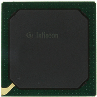
PEB20256E-V21 Infineon Technologies, PEB20256E-V21 Datasheet - Page 29

PEB20256E-V21
Manufacturer Part Number
PEB20256E-V21
Description
IC CONTROLLER INTERFACE 388-BGA
Manufacturer
Infineon Technologies
Datasheet
1.PEB20256E-V21.pdf
(232 pages)
Specifications of PEB20256E-V21
Function
Multichannel Network Interface Controller (MUNICH)
Interface
HDLC, PPP, Serial, TMA
Voltage - Supply
3 V ~ 3.6 V
Current - Supply
200mA
Power (watts)
3W
Operating Temperature
0°C ~ 70°C
Mounting Type
Surface Mount
Package / Case
388-BBGA
Lead Free Status / RoHS Status
Contains lead / RoHS non-compliant
Number Of Circuits
-
Other names
PEB20256E-V21
PEB20256E-V21IN
PEB20256E-V21IN
Available stocks
Company
Part Number
Manufacturer
Quantity
Price
Company:
Part Number:
PEB20256E-V21
Manufacturer:
MAX
Quantity:
63
Company:
Part Number:
PEB20256E-V21
Manufacturer:
Infineon Technologies
Quantity:
10 000
- Current page: 29 of 232
- Download datasheet (3Mb)
Data Sheet
V3, AA4, AD7,
AE9
AF4
Pin No.
C/BE(3:0)
PAR
Symbol
Output (O)
Input (I)
t/s
t/s
29
Command/Byte Enable
During
transaction, C/BE(3:0) define the bus
command. During the data phase, C/
BE(3:0) are used as byte enable lines.
The byte enable lines are valid for the
entire data phase and determine which
byte lanes carry meaningful data. C/BE(0)
applies to byte 0 (LSB) and C/BE(3)
applies to byte 3 (MSB).
When the MUNICH256 is bus master, C/
BE(3:0) are outputs.
When the MUNICH256 is bus slave, C/
BE(3:0) are inputs.
C/BE(3:0)
MUNICH256 is not involved in the current
transaction.
C/BE(3:0) are updated and sampled on
the rising edge of CLK.
Parity
PAR is even parity across AD(31:0) and
C/BE(3:0). PAR is stable and valid one
clock after the address phase. PAR has
the same timing as AD(31:0) but delayed
by one clock.
When the MUNICH256 i s Master, PAR is
output during address phase and write
data phases and input during read data
phase. When the MUNICH256 i s Slave,
PAR is output during read data phase and
input during write data phase.
PAR is tri-stated when the MUNICH256 is
not involved in the current transaction.
Parity errors detected by the device are
indicated on PERR output.
PAR is updated and sampled on the rising
edge of CLK.
the
are
address
Function
tri-stated
Pin Description
phase
PEB 20256 E
PEF 20256 E
when
04.2001
of
the
a
Related parts for PEB20256E-V21
Image
Part Number
Description
Manufacturer
Datasheet
Request
R

Part Number:
Description:
Manufacturer:
Infineon Technologies AG
Datasheet:

Part Number:
Description:
Manufacturer:
Infineon Technologies AG
Datasheet:

Part Number:
Description:
Manufacturer:
Infineon Technologies AG
Datasheet:

Part Number:
Description:
Manufacturer:
Infineon Technologies AG
Datasheet:

Part Number:
Description:
Manufacturer:
Infineon Technologies AG
Datasheet:

Part Number:
Description:
Manufacturer:
Infineon Technologies AG
Datasheet:

Part Number:
Description:
Manufacturer:
Infineon Technologies AG
Datasheet:

Part Number:
Description:
16-bit microcontroller with 2x2 KByte RAM
Manufacturer:
Infineon Technologies AG
Datasheet:

Part Number:
Description:
NPN silicon RF transistor
Manufacturer:
Infineon Technologies AG
Datasheet:

Part Number:
Description:
NPN silicon RF transistor
Manufacturer:
Infineon Technologies AG
Datasheet:

Part Number:
Description:
NPN silicon RF transistor
Manufacturer:
Infineon Technologies AG
Datasheet:

Part Number:
Description:
NPN silicon RF transistor
Manufacturer:
Infineon Technologies AG
Datasheet:

Part Number:
Description:
Si-MMIC-amplifier in SIEGET 25-technologie
Manufacturer:
Infineon Technologies AG
Datasheet:

Part Number:
Description:
IGBT Power Module
Manufacturer:
Infineon Technologies AG
Datasheet:

Part Number:
Description:
IC for switching-mode power supplies
Manufacturer:
Infineon Technologies AG
Datasheet:


