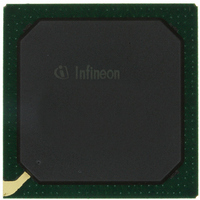
PEB20256E-V21 Infineon Technologies, PEB20256E-V21 Datasheet - Page 102

PEB20256E-V21
Manufacturer Part Number
PEB20256E-V21
Description
IC CONTROLLER INTERFACE 388-BGA
Manufacturer
Infineon Technologies
Datasheet
1.PEB20256E-V21.pdf
(232 pages)
Specifications of PEB20256E-V21
Function
Multichannel Network Interface Controller (MUNICH)
Interface
HDLC, PPP, Serial, TMA
Voltage - Supply
3 V ~ 3.6 V
Current - Supply
200mA
Power (watts)
3W
Operating Temperature
0°C ~ 70°C
Mounting Type
Surface Mount
Package / Case
388-BBGA
Lead Free Status / RoHS Status
Contains lead / RoHS non-compliant
Number Of Circuits
-
Other names
PEB20256E-V21
PEB20256E-V21IN
PEB20256E-V21IN
Available stocks
Company
Part Number
Manufacturer
Quantity
Price
Company:
Part Number:
PEB20256E-V21
Manufacturer:
MAX
Quantity:
63
Company:
Part Number:
PEB20256E-V21
Manufacturer:
Infineon Technologies
Quantity:
10 000
- Current page: 102 of 232
- Download datasheet (3Mb)
5.3.1
5.3.1.1
In Intel slave mode the bus interface supports 16-bit transactions in demultiplexed bus
operation. It uses the local bus port pins LA(12:1) for the 16 bit address and the local bus
port pins LD(15:0) for 16 bit data. A read/write access is initiated by placing an address
on the address bus and asserting LCS0 (Figure 5-5). The external processor then
activates the respective command signal (LRD, LWR). Data is driven onto the data bus
either by the MUNICH256 (for read cycles) or by the external processor (for write cycles).
After a period of time, which is determined by the access time to the internal registers
valid data is placed on the bus, which is indicated by asserting the active low signal
LRDY.
Note: LCS0 need not be deasserted between two subsequent cycles to the same
Read cycles
Input data can be latched and the command signal can be deactivated now. This causes
the MUNICH256 to remove its data from the data bus which is then tri-stated again.
LRDY is driven high and will be tri-stated as soon as LCS0 is deasserted.
Write cycles
The command signal can be deactivated now. If a subsequent bus cycle is required, the
external processor can place the respective address on the address bus.
5.3.1.2
A read/write access from the PCI bus to the 16 bit demultiplexed local bus is initiated by
accessing the PCI memory space base which is controlled by the base address
register 2. Each valid read or write access to this base address triggers the local bus
master interface which in turn starts arbitration for the local bus by asserting LHOLD (see
(1) in
asserted) it starts the local bus latency timer and begins a read/write transaction as the
bus master. The signal LHOLD remains asserted while a transaction is in progress or as
long as the local bus latency timer is not expired. A read/write transaction begins when
the MUNICH256 places a valid address on the address bus, sets the LBHE signal which
indicates a 8- or 16-bit bus access and asserts the chip select signals LCS1 and/or
LCS2. Then the MUNICH256 activates the respective command signals (LRD, LWR).
Data is driven onto the data bus either by the MUNICH256 (for write cycles) or by the
accessed device (for read cycles).
A transaction is finished on the local bus when the external device asserts LRDY (ready
controlled bus cycles) or when the internal wait state timer expires.
Data Sheet
device.
Figure5-6
Intel Mode
Slave Mode
Master Mode
). As soon as the MUNICH256 gets access to the local bus (LHLDA
102
Interface Description
PEB 20256 E
PEF 20256 E
04.2001
Related parts for PEB20256E-V21
Image
Part Number
Description
Manufacturer
Datasheet
Request
R

Part Number:
Description:
Manufacturer:
Infineon Technologies AG
Datasheet:

Part Number:
Description:
Manufacturer:
Infineon Technologies AG
Datasheet:

Part Number:
Description:
Manufacturer:
Infineon Technologies AG
Datasheet:

Part Number:
Description:
Manufacturer:
Infineon Technologies AG
Datasheet:

Part Number:
Description:
Manufacturer:
Infineon Technologies AG
Datasheet:

Part Number:
Description:
Manufacturer:
Infineon Technologies AG
Datasheet:

Part Number:
Description:
Manufacturer:
Infineon Technologies AG
Datasheet:

Part Number:
Description:
16-bit microcontroller with 2x2 KByte RAM
Manufacturer:
Infineon Technologies AG
Datasheet:

Part Number:
Description:
NPN silicon RF transistor
Manufacturer:
Infineon Technologies AG
Datasheet:

Part Number:
Description:
NPN silicon RF transistor
Manufacturer:
Infineon Technologies AG
Datasheet:

Part Number:
Description:
NPN silicon RF transistor
Manufacturer:
Infineon Technologies AG
Datasheet:

Part Number:
Description:
NPN silicon RF transistor
Manufacturer:
Infineon Technologies AG
Datasheet:

Part Number:
Description:
Si-MMIC-amplifier in SIEGET 25-technologie
Manufacturer:
Infineon Technologies AG
Datasheet:

Part Number:
Description:
IGBT Power Module
Manufacturer:
Infineon Technologies AG
Datasheet:

Part Number:
Description:
IC for switching-mode power supplies
Manufacturer:
Infineon Technologies AG
Datasheet:


