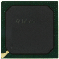
PEB20256E-V21 Infineon Technologies, PEB20256E-V21 Datasheet - Page 113

PEB20256E-V21
Manufacturer Part Number
PEB20256E-V21
Description
IC CONTROLLER INTERFACE 388-BGA
Manufacturer
Infineon Technologies
Datasheet
1.PEB20256E-V21.pdf
(232 pages)
Specifications of PEB20256E-V21
Function
Multichannel Network Interface Controller (MUNICH)
Interface
HDLC, PPP, Serial, TMA
Voltage - Supply
3 V ~ 3.6 V
Current - Supply
200mA
Power (watts)
3W
Operating Temperature
0°C ~ 70°C
Mounting Type
Surface Mount
Package / Case
388-BBGA
Lead Free Status / RoHS Status
Contains lead / RoHS non-compliant
Number Of Circuits
-
Other names
PEB20256E-V21
PEB20256E-V21IN
PEB20256E-V21IN
Available stocks
Company
Part Number
Manufacturer
Quantity
Price
Company:
Part Number:
PEB20256E-V21
Manufacturer:
MAX
Quantity:
63
Company:
Part Number:
PEB20256E-V21
Manufacturer:
Infineon Technologies
Quantity:
10 000
- Current page: 113 of 232
- Download datasheet (3Mb)
•
Figure 5-15
If no boundary scan operation is planned TRST has to be connected with V
TDI do not need to be connected since pull- up transistors ensure high input levels in this
case. Nevertheless it would be a good practice to put the unused inputs to defined levels.
In this case, if the JTAG is not used:
TMS = TCK = ‘1’ is recommended.
Test handling (boundary scan operation) is performed via the pins TCK (Test Clock),
TMS (Test Mode Select), TDI (Test Data Input) and TDO (Test Data Output) when the
TAP controller is not in its reset state, i. e. TRST is connected to V
unconnected due to its internal pull up. Test data at TDI are loaded with a clock signal
connected to TCK. ‘1’ or ‘0’ on TMS causes a transition from one controller state to
another; constant ‘1’ on TMS leads to normal operation of the chip.
An input pin (I) uses one boundary scan cell (data in), an output pin (O) uses two cells
(data out, enable) and an I/O-pin (I/O) uses three cells (data in, data out, enable). Note
that most functional output and input pins of the MUNICH256 are tested as I/O pins in
boundary scan, hence using three cells. The boundary scan unit of the MUNICH256
contains a total of n = 484 scan cells. The desired test mode is selected by serially
loading a 4-bit instruction code into the instruction register via TDI (LSB first).
EXTEST is used to examine the interconnection of the devices on the board. In this test
mode at first all input pins capture the current level on the corresponding external
interconnection line, whereas all output pins are held at constant values (‘0’ or ‘1’). Then
the contents of the boundary scan is shifted to TDO. At the same time the next scan
vector is loaded from TDI. Subsequently all output pins are updated according to the new
Data Sheet
Block Diagram of Test Access Port and Boundary Scan Unit
TCK
TRST
TMS
TDI
TDO
CLOCK
Reset
Test
Control
Data in
Enable
Data out
Test Access Port (TAP)
- Finite State Machine
- Instruction Register (4 bit)
- Test Signal Generator
Clock Generation
TAP Controller
CLOCK
113
ID Data out
Control
Bus
SS Data
out
Interface Description
DD3
PEB 20256 E
2
PEF 20256 E
1
n
Pins
.
.
.
.
.
.
or it remains
SS
. TMS and
04.2001
Related parts for PEB20256E-V21
Image
Part Number
Description
Manufacturer
Datasheet
Request
R

Part Number:
Description:
Manufacturer:
Infineon Technologies AG
Datasheet:

Part Number:
Description:
Manufacturer:
Infineon Technologies AG
Datasheet:

Part Number:
Description:
Manufacturer:
Infineon Technologies AG
Datasheet:

Part Number:
Description:
Manufacturer:
Infineon Technologies AG
Datasheet:

Part Number:
Description:
Manufacturer:
Infineon Technologies AG
Datasheet:

Part Number:
Description:
Manufacturer:
Infineon Technologies AG
Datasheet:

Part Number:
Description:
Manufacturer:
Infineon Technologies AG
Datasheet:

Part Number:
Description:
16-bit microcontroller with 2x2 KByte RAM
Manufacturer:
Infineon Technologies AG
Datasheet:

Part Number:
Description:
NPN silicon RF transistor
Manufacturer:
Infineon Technologies AG
Datasheet:

Part Number:
Description:
NPN silicon RF transistor
Manufacturer:
Infineon Technologies AG
Datasheet:

Part Number:
Description:
NPN silicon RF transistor
Manufacturer:
Infineon Technologies AG
Datasheet:

Part Number:
Description:
NPN silicon RF transistor
Manufacturer:
Infineon Technologies AG
Datasheet:

Part Number:
Description:
Si-MMIC-amplifier in SIEGET 25-technologie
Manufacturer:
Infineon Technologies AG
Datasheet:

Part Number:
Description:
IGBT Power Module
Manufacturer:
Infineon Technologies AG
Datasheet:

Part Number:
Description:
IC for switching-mode power supplies
Manufacturer:
Infineon Technologies AG
Datasheet:


