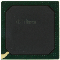
PEB20256E-V21 Infineon Technologies, PEB20256E-V21 Datasheet - Page 100

PEB20256E-V21
Manufacturer Part Number
PEB20256E-V21
Description
IC CONTROLLER INTERFACE 388-BGA
Manufacturer
Infineon Technologies
Datasheet
1.PEB20256E-V21.pdf
(232 pages)
Specifications of PEB20256E-V21
Function
Multichannel Network Interface Controller (MUNICH)
Interface
HDLC, PPP, Serial, TMA
Voltage - Supply
3 V ~ 3.6 V
Current - Supply
200mA
Power (watts)
3W
Operating Temperature
0°C ~ 70°C
Mounting Type
Surface Mount
Package / Case
388-BBGA
Lead Free Status / RoHS Status
Contains lead / RoHS non-compliant
Number Of Circuits
-
Other names
PEB20256E-V21
PEB20256E-V21IN
PEB20256E-V21IN
Available stocks
Company
Part Number
Manufacturer
Quantity
Price
Company:
Part Number:
PEB20256E-V21
Manufacturer:
MAX
Quantity:
63
Company:
Part Number:
PEB20256E-V21
Manufacturer:
Infineon Technologies
Quantity:
10 000
- Current page: 100 of 232
- Download datasheet (3Mb)
address is sent, the data stored in the memory at the selected address is shifted in on
the SPSI pin. The read operation is terminated by setting SPCS high (see Figure 5-3).
•
Figure 5-3
5.2.3
Prior to any attempt to write data to an external EEPROM, the write enable latch must
be set by issuing the WREN instruction. This is done by setting SPCS low and then
clocking out the WREN instruction. After all eight bits of the instruction are transmitted,
the SPCS will be brought high to set the write enable latch.
Once the write enable latch is set, the user may proceed by issuing a write instruction,
followed by the eight bit address and then the data to be written. In order that data will
actually be written to the EEPROM, the SPCS is set high after the least significant bit
(D0) of the data byte has been clocked in. Refer to Figure 5-4 for detailed illustrations
on the byte write sequence. While the write is in progress, the register bit SPI.START
may be read to check the status of the transaction. When a write cycle is completed, the
register bit SPI.START is reset.
•
Figure 5-4
Data Sheet
SPCLK
SPCLK
SPCS
SPSO
SPCS
SPSO
SPSI
SPSI
SPI Write Sequence
SPI Read Sequence
SPI Write Sequence
0
0
0
0
1
0
1
0
2
0
2
0
instruction
instruction
3
0
3
0
4
0
4
0
5
0
5
0
6
1
6
1
7
1
7
0
100
8
8
7
7
9
9
6
6
8 bit address
8 bit address
14 15 16 17 18 19 20 21 22 23
14 15 16 17 18 19 20 21 22 23
0
0
7
7
6
6
Interface Description
5
5
data out
data in
4
4
3
3
PEB 20256 E
PEF 20256 E
2
2
1
1
0
0
04.2001
Related parts for PEB20256E-V21
Image
Part Number
Description
Manufacturer
Datasheet
Request
R

Part Number:
Description:
Manufacturer:
Infineon Technologies AG
Datasheet:

Part Number:
Description:
Manufacturer:
Infineon Technologies AG
Datasheet:

Part Number:
Description:
Manufacturer:
Infineon Technologies AG
Datasheet:

Part Number:
Description:
Manufacturer:
Infineon Technologies AG
Datasheet:

Part Number:
Description:
Manufacturer:
Infineon Technologies AG
Datasheet:

Part Number:
Description:
Manufacturer:
Infineon Technologies AG
Datasheet:

Part Number:
Description:
Manufacturer:
Infineon Technologies AG
Datasheet:

Part Number:
Description:
16-bit microcontroller with 2x2 KByte RAM
Manufacturer:
Infineon Technologies AG
Datasheet:

Part Number:
Description:
NPN silicon RF transistor
Manufacturer:
Infineon Technologies AG
Datasheet:

Part Number:
Description:
NPN silicon RF transistor
Manufacturer:
Infineon Technologies AG
Datasheet:

Part Number:
Description:
NPN silicon RF transistor
Manufacturer:
Infineon Technologies AG
Datasheet:

Part Number:
Description:
NPN silicon RF transistor
Manufacturer:
Infineon Technologies AG
Datasheet:

Part Number:
Description:
Si-MMIC-amplifier in SIEGET 25-technologie
Manufacturer:
Infineon Technologies AG
Datasheet:

Part Number:
Description:
IGBT Power Module
Manufacturer:
Infineon Technologies AG
Datasheet:

Part Number:
Description:
IC for switching-mode power supplies
Manufacturer:
Infineon Technologies AG
Datasheet:


