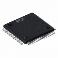
SAA7115HL/V1,518 NXP Semiconductors, SAA7115HL/V1,518 Datasheet - Page 524

SAA7115HL/V1,518
Manufacturer Part Number
SAA7115HL/V1,518
Description
IC DIGITAL VIDEO DECODER 100LQFP
Manufacturer
NXP Semiconductors
Type
Video Decoderr
Specifications of SAA7115HL/V1,518
Package / Case
100-LQFP
Applications
Set-Top Boxes
Mounting Type
Surface Mount
Mounting Style
SMD/SMT
Lead Free Status / RoHS Status
Lead free / RoHS Compliant
Voltage - Supply, Analog
-
Voltage - Supply, Digital
-
Lead Free Status / RoHS Status
Lead free / RoHS Compliant, Lead free / RoHS Compliant
Other names
935270666518
SAA7115HLBE-T
SAA7115HLBE-T
SAA7115HLBE-T
SAA7115HLBE-T
Available stocks
Company
Part Number
Manufacturer
Quantity
Price
Company:
Part Number:
SAA7115HL/V1,518
Manufacturer:
Sigma Designs Inc
Quantity:
10 000
- Current page: 524 of 548
- Download datasheet (6Mb)
PNX1300/01/02/11 Data Book
bit and the BSX bit in the PCSW register should the
same. This byte sex bit must be set by the software.
Figure C-14
mat as seen in the SDRAM and highway bus. The input
data is byte oriented and no swapping is required in the
VLD unit.
DSPCPU in words, thus the VLD needs to swap the out-
put bytes within a word (shown in
pensate for the CPU swap.
C-8
Figure C-13. Memory image format for audio data
Figure C-15. SSI data format as seen in highway
lsb is the least significant byte
msb is the most significant byte
8-bit data (mono)
in memory
8-bit data (stereo)
in memory
32-bit data
in memory
16-bit data (mono)
in memory
16-bit data (stereo)
in memory
lsb is the least significant byte
msb is the most significant byte
16-bit half-word data
in CPU/MMIOs
describes the VLD input and output data for-
However, the output data is read by the
PRELIMINARY SPECIFICATION
lsb
lsb
lsb
msb
L
R
A+3
A+3
A+3
A+3
A+3
n+3
A+3
n+1
L
R
Figure
D
n+1
n
n
SSI_CTL.EMS = 0
Big Endian Mode
A+2
L
L
A+2
A+2
A+2
A+2
A+2
n+2
n+1
msb
msb
C-14) to com-
lsb
lsb
lsb
msb
A+1
L
A+1
R
A+1
A+1
A+1
A+1
n+1
n
D
and A+3 corresponds to byte-three lane of SDRAM/Hwy
and A+3 corresponds to byte-3 lane of CPU/Hwy
Note: A+0 corresponds to byte-zero lane of SDRAM/Hwy
Note: A+0 corresponds to byte-0 lane of CPU/Hwy
L
L
n+1
n
n
A+0
A+0
A+0
A+0
A+0
L
L
A+0
C.4.8
The SSI unit has I/O connections through the external
serial pins and also to the internal 32-bit data highway via
MMIO transactions. The minimum quantity of data to be
analyzed by the CPU is 16-bits (i.e. one half word). The
SSI uses a 16-bit or 1-bit endian-ness; it is detailed in
Section 17.8 on page
in the CPU register is written or read ‘as is’ into/from the
SSI MMIO register. The EMS bit in SSI_CTL determines
which half-word (16-bit) is sent first as pictured in
C-15.
n
n
msb
msb
msb
lsb
Synchronous Serial Interface (SSI)
msb
msb
msb
msb
L
R
A+3
A+3
A+3
A+3
A+3
A+3
n+3
n+1
L
R
D
n+1
n
n+1
Little Endian Mode
SSI_CTL.EMS = 1
17-7. The 32-bit quantity contained
A+2
A+2
A+2
A+2
A+2
L
L
A+2
n+2
n+1
lsb
lsb
Philips Semiconductors
lsb
msb
msb
msb
A+1
A+1
L
R
A+1
A+1
A+1
A+1
n+1
n
L
L
D
n
n
n
A+0
A+0
A+0
A+0
A+0
A+0
L
L
n
n
lsb
lsb
lsb
lsb
Figure
Related parts for SAA7115HL/V1,518
Image
Part Number
Description
Manufacturer
Datasheet
Request
R

Part Number:
Description:
IC ADV DGTL VIDEO DECODR 100LQFP
Manufacturer:
NXP Semiconductors
Datasheet:

Part Number:
Description:
Video ICs ADV DGTL VIDEO DECODR
Manufacturer:
NXP Semiconductors
Datasheet:
Part Number:
Description:
Ntsc/pal/secam 9-bit Video Decoder
Manufacturer:
NXP Semiconductors
Datasheet:
Part Number:
Description:
NXP Semiconductors designed the LPC2420/2460 microcontroller around a 16-bit/32-bitARM7TDMI-S CPU core with real-time debug interfaces that include both JTAG andembedded trace
Manufacturer:
NXP Semiconductors
Datasheet:

Part Number:
Description:
NXP Semiconductors designed the LPC2458 microcontroller around a 16-bit/32-bitARM7TDMI-S CPU core with real-time debug interfaces that include both JTAG andembedded trace
Manufacturer:
NXP Semiconductors
Datasheet:
Part Number:
Description:
NXP Semiconductors designed the LPC2468 microcontroller around a 16-bit/32-bitARM7TDMI-S CPU core with real-time debug interfaces that include both JTAG andembedded trace
Manufacturer:
NXP Semiconductors
Datasheet:
Part Number:
Description:
NXP Semiconductors designed the LPC2470 microcontroller, powered by theARM7TDMI-S core, to be a highly integrated microcontroller for a wide range ofapplications that require advanced communications and high quality graphic displays
Manufacturer:
NXP Semiconductors
Datasheet:
Part Number:
Description:
NXP Semiconductors designed the LPC2478 microcontroller, powered by theARM7TDMI-S core, to be a highly integrated microcontroller for a wide range ofapplications that require advanced communications and high quality graphic displays
Manufacturer:
NXP Semiconductors
Datasheet:
Part Number:
Description:
The Philips Semiconductors XA (eXtended Architecture) family of 16-bit single-chip microcontrollers is powerful enough to easily handle the requirements of high performance embedded applications, yet inexpensive enough to compete in the market for hi
Manufacturer:
NXP Semiconductors
Datasheet:
Part Number:
Description:
The XA-S3 device is a member of Philips Semiconductors? XA(eXtended Architecture) family of high performance 16-bitsingle-chip microcontrollers
Manufacturer:
NXP Semiconductors
Datasheet:

Part Number:
Description:
The NXP BlueStreak LH75401/LH75411 family consists of two low-cost 16/32-bit System-on-Chip (SoC) devices
Manufacturer:
NXP Semiconductors
Datasheet:

Part Number:
Description:
The NXP LPC3130/3131 combine an 180 MHz ARM926EJ-S CPU core, high-speed USB2
Manufacturer:
NXP Semiconductors
Datasheet:

Part Number:
Description:
The NXP LPC3141 combine a 270 MHz ARM926EJ-S CPU core, High-speed USB 2
Manufacturer:
NXP Semiconductors


