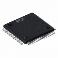
SAA7115HL/V1,518 NXP Semiconductors, SAA7115HL/V1,518 Datasheet - Page 181

SAA7115HL/V1,518
Manufacturer Part Number
SAA7115HL/V1,518
Description
IC DIGITAL VIDEO DECODER 100LQFP
Manufacturer
NXP Semiconductors
Type
Video Decoderr
Specifications of SAA7115HL/V1,518
Package / Case
100-LQFP
Applications
Set-Top Boxes
Mounting Type
Surface Mount
Mounting Style
SMD/SMT
Lead Free Status / RoHS Status
Lead free / RoHS Compliant
Voltage - Supply, Analog
-
Voltage - Supply, Digital
-
Lead Free Status / RoHS Status
Lead free / RoHS Compliant, Lead free / RoHS Compliant
Other names
935270666518
SAA7115HLBE-T
SAA7115HLBE-T
SAA7115HLBE-T
SAA7115HLBE-T
Available stocks
Company
Part Number
Manufacturer
Quantity
Price
Company:
Part Number:
SAA7115HL/V1,518
Manufacturer:
Sigma Designs Inc
Quantity:
10 000
- Current page: 181 of 548
- Download datasheet (6Mb)
Philips Semiconductors
Figure 11-13. Back-to-back PCI burst write operations with 16 data phases which might be generated by the
ICP when writing image data to a PCI-resident video frame buffer.
11.8
11.8.1
The PCI interface does not implement lock#, sbo, and
sbone pins. Consequently, it is possible for both the
DSPCPU and external PCI initiators to write to a critical
memory section simultaneously. Software must imple-
ment policies to guarantee memory coherency.
11.8.2
PNX1300 does not implement the PCI expansion ROM
capability.
Figure 11-12. PCI burst write operation with 16 data phases.
LIMITATIONS
Bus Locking
No Expansion ROM
devsel#
frame#
pci_clk
c/be#
trdy#
irdy#
ad
devsel#
frame#
pci_clk
c/be#
trdy#
irdy#
ad
1
Command
Address
1
2
Command
Address
2
Data 1
3
Data 1
3
Byte Enables
Data 2
Data 15
4
18
Data 3
Data 16
5
11.8.3
The PCI interface does not implement the PCI cacheline-
wrap address mode for external PCI initiators that ac-
cess PNX1300 SDRAM.
11.8.4
Only single-data-phase transactions to configuration and
I/O spaces are supported. The byte-enable signals se-
lect the byte(s) within the addressed word.
11.8.5
External initiators can access PNX1300 MMIO registers
only as full words. The byte-enable signals have no ef-
fect on the data transferred. External initiators must read
and write all four bytes of MMIO registers.
PRELIMINARY SPECIFICATION
19
Byte Enables
Data 4
Data 17
6
20
No Cacheline Wrap Address
Sequence
No Burst for I/O or Configuration
Space
Word-Only MMIO Register Access
Byte Enables
Data 15
17
Data 31
35
Data 16
18
Data 32
36
PCI Interface
11-17
Related parts for SAA7115HL/V1,518
Image
Part Number
Description
Manufacturer
Datasheet
Request
R

Part Number:
Description:
IC ADV DGTL VIDEO DECODR 100LQFP
Manufacturer:
NXP Semiconductors
Datasheet:

Part Number:
Description:
Video ICs ADV DGTL VIDEO DECODR
Manufacturer:
NXP Semiconductors
Datasheet:
Part Number:
Description:
Ntsc/pal/secam 9-bit Video Decoder
Manufacturer:
NXP Semiconductors
Datasheet:
Part Number:
Description:
NXP Semiconductors designed the LPC2420/2460 microcontroller around a 16-bit/32-bitARM7TDMI-S CPU core with real-time debug interfaces that include both JTAG andembedded trace
Manufacturer:
NXP Semiconductors
Datasheet:

Part Number:
Description:
NXP Semiconductors designed the LPC2458 microcontroller around a 16-bit/32-bitARM7TDMI-S CPU core with real-time debug interfaces that include both JTAG andembedded trace
Manufacturer:
NXP Semiconductors
Datasheet:
Part Number:
Description:
NXP Semiconductors designed the LPC2468 microcontroller around a 16-bit/32-bitARM7TDMI-S CPU core with real-time debug interfaces that include both JTAG andembedded trace
Manufacturer:
NXP Semiconductors
Datasheet:
Part Number:
Description:
NXP Semiconductors designed the LPC2470 microcontroller, powered by theARM7TDMI-S core, to be a highly integrated microcontroller for a wide range ofapplications that require advanced communications and high quality graphic displays
Manufacturer:
NXP Semiconductors
Datasheet:
Part Number:
Description:
NXP Semiconductors designed the LPC2478 microcontroller, powered by theARM7TDMI-S core, to be a highly integrated microcontroller for a wide range ofapplications that require advanced communications and high quality graphic displays
Manufacturer:
NXP Semiconductors
Datasheet:
Part Number:
Description:
The Philips Semiconductors XA (eXtended Architecture) family of 16-bit single-chip microcontrollers is powerful enough to easily handle the requirements of high performance embedded applications, yet inexpensive enough to compete in the market for hi
Manufacturer:
NXP Semiconductors
Datasheet:
Part Number:
Description:
The XA-S3 device is a member of Philips Semiconductors? XA(eXtended Architecture) family of high performance 16-bitsingle-chip microcontrollers
Manufacturer:
NXP Semiconductors
Datasheet:

Part Number:
Description:
The NXP BlueStreak LH75401/LH75411 family consists of two low-cost 16/32-bit System-on-Chip (SoC) devices
Manufacturer:
NXP Semiconductors
Datasheet:

Part Number:
Description:
The NXP LPC3130/3131 combine an 180 MHz ARM926EJ-S CPU core, high-speed USB2
Manufacturer:
NXP Semiconductors
Datasheet:

Part Number:
Description:
The NXP LPC3141 combine a 270 MHz ARM926EJ-S CPU core, High-speed USB 2
Manufacturer:
NXP Semiconductors


