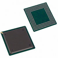
DS3134 Maxim Integrated Products, DS3134 Datasheet - Page 183

DS3134
Manufacturer Part Number
DS3134
Description
IC CTRLR HDLC CHATEAU 256-BGA
Manufacturer
Maxim Integrated Products
Datasheet
1.DS3134.pdf
(203 pages)
Specifications of DS3134
Controller Type
HDLC Controller
Interface
Serial
Voltage - Supply
3 V ~ 3.6 V
Current - Supply
500mA
Operating Temperature
0°C ~ 70°C
Mounting Type
Surface Mount
Package / Case
256-BGA
Lead Free Status / RoHS Status
Contains lead / RoHS non-compliant
Available stocks
Company
Part Number
Manufacturer
Quantity
Price
Company:
Part Number:
DS3134
Manufacturer:
DALLAS
Quantity:
1 831
Company:
Part Number:
DS3134 (BGA256)
Manufacturer:
DALLAS
Quantity:
246
- Current page: 183 of 203
- Download datasheet (778Kb)
DS3134
SAMPLE/PRELOAD
A mandatory instruction for the IEEE 1149.1 specification. This instruction supports two functions. The
digital I/Os of the DS3134 can be sampled at the Boundary Scan register without interfering with the
normal operation of the device by using the Capture-DR state. SAMPLE/PRELOAD also allows the
DS3134 to shift data into the Boundary Scan register via JTDI using the Shift-DR state.
EXTEST
EXTEST allows testing of all interconnections to the DS3134. When the EXTEST instruction is latched
in the instruction register, the following actions occur. Once enabled via the Update-IR state, the parallel
outputs of all digital output pins will be driven. The Boundary Scan register will be connected between
JTDI and JTDO. The Capture-DR will sample digital inputs into the Boundary Scan register.
BYPASS
When the BYPASS instruction is latched into the parallel Instruction register, JTDI connects to JTDO
through the one-bit Bypass Test register. This allows data to pass from JTDI to JTDO not affecting the
device's normal operation.
IDCODE
When the IDCODE instruction is latched into the parallel Instruction register, the Identification Test
register is selected. The device identification code will be loaded into the Identification register on the
rising edge of JTCLK following entry into the Capture-DR state. Shift-DR can be used to shift the
identification code out serially via JTDO. During Test-Logic-Reset, the identification code is forced into
the instruction register's parallel output. The device ID code will always have a one in the LSB position.
The next 11 bits identify the manufacturer's JEDEC number and number of continuation bytes followed
by 16 bits for the device and 4 bits for the version. The device ID code for the DS3134 is 00006143h.
11.4 TEST REGISTERS
IEEE 1149.1 requires a minimum of two Test registers; the Bypass register and the Boundary Scan
register. An optional Test register has been included in the DS3134 design. This Test register is the
Identification register and is used in conjunction with the IDCODE instruction and the Test-Logic-Reset
state of the TAP controller.
Bypass Register
This is a single one-bit shift register used in conjunction with the BYPASS, CLAMP, and HIGHZ
instructions, which provides a short path between JTDI and JTDO.
Identification Register
The Identification register contains a 32-bit shift register and a 32-bit latched parallel output. This
register is selected during the IDCODE instruction and when the TAP controller is in the Test-Logic-
Reset state.
Boundary Scan Register
This register contains both a shift register path and a latched parallel output for all control cells and digital
I/O cells and is TBD bits in length. Table 11.4A shows all of the cell bit locations and definitions.
183 of 203
Related parts for DS3134
Image
Part Number
Description
Manufacturer
Datasheet
Request
R

Part Number:
Description:
MAX7528KCWPMaxim Integrated Products [CMOS Dual 8-Bit Buffered Multiplying DACs]
Manufacturer:
Maxim Integrated Products
Datasheet:

Part Number:
Description:
Single +5V, fully integrated, 1.25Gbps laser diode driver.
Manufacturer:
Maxim Integrated Products
Datasheet:

Part Number:
Description:
Single +5V, fully integrated, 155Mbps laser diode driver.
Manufacturer:
Maxim Integrated Products
Datasheet:

Part Number:
Description:
VRD11/VRD10, K8 Rev F 2/3/4-Phase PWM Controllers with Integrated Dual MOSFET Drivers
Manufacturer:
Maxim Integrated Products
Datasheet:

Part Number:
Description:
Highly Integrated Level 2 SMBus Battery Chargers
Manufacturer:
Maxim Integrated Products
Datasheet:

Part Number:
Description:
Current Monitor and Accumulator with Integrated Sense Resistor; ; Temperature Range: -40°C to +85°C
Manufacturer:
Maxim Integrated Products

Part Number:
Description:
TSSOP 14/A�/RS-485 Transceivers with Integrated 100O/120O Termination Resis
Manufacturer:
Maxim Integrated Products

Part Number:
Description:
TSSOP 14/A�/RS-485 Transceivers with Integrated 100O/120O Termination Resis
Manufacturer:
Maxim Integrated Products

Part Number:
Description:
QFN 16/A�/AC-DC and DC-DC Peak-Current-Mode Converters with Integrated Step
Manufacturer:
Maxim Integrated Products

Part Number:
Description:
TDFN/A/65V, 1A, 600KHZ, SYNCHRONOUS STEP-DOWN REGULATOR WITH INTEGRATED SWI
Manufacturer:
Maxim Integrated Products

Part Number:
Description:
Integrated Temperature Controller f
Manufacturer:
Maxim Integrated Products

Part Number:
Description:
SOT23-6/I�/45MHz to 650MHz, Integrated IF VCOs with Differential Output
Manufacturer:
Maxim Integrated Products

Part Number:
Description:
SOT23-6/I�/45MHz to 650MHz, Integrated IF VCOs with Differential Output
Manufacturer:
Maxim Integrated Products

Part Number:
Description:
EVALUATION KIT/2.4GHZ TO 2.5GHZ 802.11G/B RF TRANSCEIVER WITH INTEGRATED PA
Manufacturer:
Maxim Integrated Products

Part Number:
Description:
QFN/E/DUAL PCIE/SATA HIGH SPEED SWITCH WITH INTEGRATED BIAS RESISTOR
Manufacturer:
Maxim Integrated Products
Datasheet:


