DS3134 Maxim Integrated Products, DS3134 Datasheet - Page 147

DS3134
Manufacturer Part Number
DS3134
Description
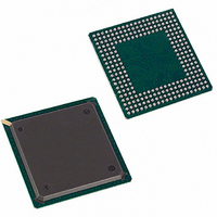
IC CTRLR HDLC CHATEAU 256-BGA
Manufacturer
Maxim Integrated Products
Datasheet
1.DS3134.pdf
(203 pages)
Specifications of DS3134
Controller Type
HDLC Controller
Interface
Serial
Voltage - Supply
3 V ~ 3.6 V
Current - Supply
500mA
Operating Temperature
0°C ~ 70°C
Mounting Type
Surface Mount
Package / Case
256-BGA
Lead Free Status / RoHS Status
Contains lead / RoHS non-compliant
Available stocks
Company
Part Number
Manufacturer
Quantity
Price
Company:
Part Number:
DS3134
Manufacturer:
DALLAS
Quantity:
1 831
Company:
Part Number:
DS3134 (BGA256)
Manufacturer:
DALLAS
Quantity:
246
- Current page: 147 of 203
- Download datasheet (778Kb)
PCI Write Cycle
A write cycle on the PCI bus is shown in Figure 9.1C. During clock cycle #1, the initiator asserts the
PFRAME* signal and drives the address onto the PAD signal lines and the bus command (which would
be a write) onto the PCBE* signal lines. The target reads the address and bus command and if the address
matches it's own, then it will assert the PDEVSEL* signal and begin the bus transaction. During clock
cycle #2, the initiator stops driving the address onto the PAD signal lines and begins driving data #1. It
also switches the PCBE* signal lines to now indicate the byte enable for data #1. The initiator asserts the
PIRDY* signal and begins monitoring the PDEVSEL* and PTRDY* signals. During clock cycle #3, the
initiator detects that PDEVSEL* and PTRDY* are asserted which indicates that the target has accepted
data #1 and the initiator begins driving the data and byte enable for data #2. During clock cycle #4, since
PDEVSEL* and PTRDY* are asserted, data #2 is written by the initiator to the target. During clock cycle
#5, both PIRDY* and PTRDY* are deasserted indicating that neither the initiator nor the target are ready
for data #3 to be passed. During clock cycle #6, the initiator is now ready so it asserts PIRDY* and
deasserts PFRAME* which indicates that data #3 will be the last one passed. During clock cycle #8, the
target asserts PTRDY* which indicates to the initiator that data #3 is ready to be accepted by the target.
During clock cycle #9, the initiator deasserts PIRDY* and stops driving the PAD and PCBE* signal lines.
The target deasserts PDEVSEL* and PTRDY*.
The PXAS*, PXDS*, and PXBLAST* signals are not part of a standard PCI bus. These PCI extension
signals that are unique to the device. They are useful in adapting the PCI bus to a proprietary bus scheme.
They are only asserted when the device is a bus master.
PCI Bus Write Figure 9.1C
PCLK
PFRAME*
PAD
PCBE*
PIRDY*
PTRDY*
PDEVSEL*
PXAS*
PXDS*
PXBLAST*
1
Address
CMD
2
data #1
BE #1
3
4
BE #2
5
147 of 203
data #2
6
BE #3
7
data #3
8
9
pci_writ
10
DS3134
Related parts for DS3134
Image
Part Number
Description
Manufacturer
Datasheet
Request
R

Part Number:
Description:
MAX7528KCWPMaxim Integrated Products [CMOS Dual 8-Bit Buffered Multiplying DACs]
Manufacturer:
Maxim Integrated Products
Datasheet:

Part Number:
Description:
Single +5V, fully integrated, 1.25Gbps laser diode driver.
Manufacturer:
Maxim Integrated Products
Datasheet:

Part Number:
Description:
Single +5V, fully integrated, 155Mbps laser diode driver.
Manufacturer:
Maxim Integrated Products
Datasheet:

Part Number:
Description:
VRD11/VRD10, K8 Rev F 2/3/4-Phase PWM Controllers with Integrated Dual MOSFET Drivers
Manufacturer:
Maxim Integrated Products
Datasheet:

Part Number:
Description:
Highly Integrated Level 2 SMBus Battery Chargers
Manufacturer:
Maxim Integrated Products
Datasheet:

Part Number:
Description:
Current Monitor and Accumulator with Integrated Sense Resistor; ; Temperature Range: -40°C to +85°C
Manufacturer:
Maxim Integrated Products

Part Number:
Description:
TSSOP 14/A�/RS-485 Transceivers with Integrated 100O/120O Termination Resis
Manufacturer:
Maxim Integrated Products

Part Number:
Description:
TSSOP 14/A�/RS-485 Transceivers with Integrated 100O/120O Termination Resis
Manufacturer:
Maxim Integrated Products

Part Number:
Description:
QFN 16/A�/AC-DC and DC-DC Peak-Current-Mode Converters with Integrated Step
Manufacturer:
Maxim Integrated Products

Part Number:
Description:
TDFN/A/65V, 1A, 600KHZ, SYNCHRONOUS STEP-DOWN REGULATOR WITH INTEGRATED SWI
Manufacturer:
Maxim Integrated Products

Part Number:
Description:
Integrated Temperature Controller f
Manufacturer:
Maxim Integrated Products

Part Number:
Description:
SOT23-6/I�/45MHz to 650MHz, Integrated IF VCOs with Differential Output
Manufacturer:
Maxim Integrated Products

Part Number:
Description:
SOT23-6/I�/45MHz to 650MHz, Integrated IF VCOs with Differential Output
Manufacturer:
Maxim Integrated Products

Part Number:
Description:
EVALUATION KIT/2.4GHZ TO 2.5GHZ 802.11G/B RF TRANSCEIVER WITH INTEGRATED PA
Manufacturer:
Maxim Integrated Products

Part Number:
Description:
QFN/E/DUAL PCIE/SATA HIGH SPEED SWITCH WITH INTEGRATED BIAS RESISTOR
Manufacturer:
Maxim Integrated Products
Datasheet:


