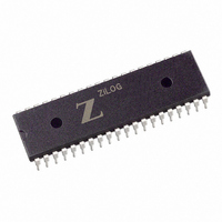
Z8523008PSG Zilog, Z8523008PSG Datasheet - Page 75

Z8523008PSG
Manufacturer Part Number
Z8523008PSG
Description
IC 8MHZ ESCC 40-DIP
Manufacturer
Zilog
Datasheet
1.Z8523008PSG.pdf
(117 pages)
Specifications of Z8523008PSG
Controller Type
Serial Communications Controller (SCC)
Interface
Bus
Voltage - Supply
4.5 V ~ 5.5 V
Current - Supply
4mA
Operating Temperature
0°C ~ 70°C
Mounting Type
Through Hole
Package / Case
40-DIP (0.620", 15.75mm)
Operating Supply Voltage
5 V
Supply Current (max)
9 mA
Maximum Operating Temperature
+ 70 C
Minimum Operating Temperature
0 C
Mounting Style
Through Hole
Lead Free Status / RoHS Status
Lead free / RoHS Compliant
Other names
269-3917
Z8523008PSG
Z8523008PSG
Available stocks
Company
Part Number
Manufacturer
Quantity
Price
Company:
Part Number:
Z8523008PSG
Manufacturer:
Zilog
Quantity:
177
- Current page: 75 of 117
- Download datasheet (2Mb)
Z80230 Interface Timing
PS005303-0907
Z80230 Write Cycle Timing
The Z-Bus compatible ESCC is suited for system applications with multiplexed address/
data buses.
Two control signals, AS and DS, are used by the Z80230 to control bus transactions. Addi-
tionally, four other control signals (CS0, CS1, RW, and INTACK) control the type of bus
transaction that occurs. A bus transaction is initiated by AS. The rising edge latches the
register address on the Address/Data bus and the state of INTACK and CS0.
In addition to bus transactions, the interrupt section uses the AS to set Interrupt Pending
(IP) bits. Therefore, AS must be kept cycling for the interrupt section to function.
The Z80230 generates internal control signals in response to a register access. Because AS
and DS have no defined phase relationship with PCLK, the circuitry generating these
internal control signals provide time for metastable conditions to disappear. This action
results in a recovery time related to PCLK.
This recovery time applies only to transactions involving the Z80230, and any intervening
transactions are ignored. This recovery time is four PCLK cycles, measured from the fall-
ing edge of DS for one access to the ESCC, to the falling edge of DS for a subsequent
access.
INTACK
A7–A0
CS0
R/W
CS1
DS
AS
Figure 17
Figure 17. Z80230 Write Cycle Timing
illustrates the Write cycle timing.
Address
Data Valid
Product Specification
Z80230 Interface Timing
Z85230/Z80230
70
Related parts for Z8523008PSG
Image
Part Number
Description
Manufacturer
Datasheet
Request
R

Part Number:
Description:
Enhanced Serial Communications Controller
Manufacturer:
ZiLOG Semiconductor
Datasheet:

Part Number:
Description:
Communication Controllers, ZILOG INTELLIGENT PERIPHERAL CONTROLLER (ZIP)
Manufacturer:
Zilog, Inc.
Datasheet:

Part Number:
Description:
KIT DEV FOR Z8 ENCORE 16K TO 64K
Manufacturer:
Zilog
Datasheet:

Part Number:
Description:
KIT DEV Z8 ENCORE XP 28-PIN
Manufacturer:
Zilog
Datasheet:

Part Number:
Description:
DEV KIT FOR Z8 ENCORE 8K/4K
Manufacturer:
Zilog
Datasheet:

Part Number:
Description:
KIT DEV Z8 ENCORE XP 28-PIN
Manufacturer:
Zilog
Datasheet:

Part Number:
Description:
DEV KIT FOR Z8 ENCORE 4K TO 8K
Manufacturer:
Zilog
Datasheet:

Part Number:
Description:
CMOS Z8 microcontroller. ROM 16 Kbytes, RAM 256 bytes, speed 16 MHz, 32 lines I/O, 3.0V to 5.5V
Manufacturer:
Zilog, Inc.
Datasheet:

Part Number:
Description:
Low-cost microcontroller. 512 bytes ROM, 61 bytes RAM, 8 MHz
Manufacturer:
Zilog, Inc.
Datasheet:

Part Number:
Description:
Z8 4K OTP Microcontroller
Manufacturer:
Zilog, Inc.
Datasheet:

Part Number:
Description:
CMOS SUPER8 ROMLESS MCU
Manufacturer:
Zilog, Inc.
Datasheet:

Part Number:
Description:
SL1866 CMOSZ8 OTP Microcontroller
Manufacturer:
Zilog, Inc.
Datasheet:

Part Number:
Description:
SL1866 CMOSZ8 OTP Microcontroller
Manufacturer:
Zilog, Inc.
Datasheet:

Part Number:
Description:
OTP (KB) = 1, RAM = 125, Speed = 12, I/O = 14, 8-bit Timers = 2, Comm Interfaces Other Features = Por, LV Protect, Voltage = 4.5-5.5V
Manufacturer:
Zilog, Inc.
Datasheet:


