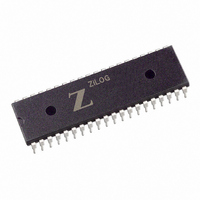
Z8523008PSG Zilog, Z8523008PSG Datasheet - Page 37

Z8523008PSG
Manufacturer Part Number
Z8523008PSG
Description
IC 8MHZ ESCC 40-DIP
Manufacturer
Zilog
Datasheet
1.Z8523008PSG.pdf
(117 pages)
Specifications of Z8523008PSG
Controller Type
Serial Communications Controller (SCC)
Interface
Bus
Voltage - Supply
4.5 V ~ 5.5 V
Current - Supply
4mA
Operating Temperature
0°C ~ 70°C
Mounting Type
Through Hole
Package / Case
40-DIP (0.620", 15.75mm)
Operating Supply Voltage
5 V
Supply Current (max)
9 mA
Maximum Operating Temperature
+ 70 C
Minimum Operating Temperature
0 C
Mounting Style
Through Hole
Lead Free Status / RoHS Status
Lead free / RoHS Compliant
Other names
269-3917
Z8523008PSG
Z8523008PSG
Available stocks
Company
Part Number
Manufacturer
Quantity
Price
Company:
Part Number:
Z8523008PSG
Manufacturer:
Zilog
Quantity:
177
Programming
PS005303-0907
Initializing
Write Registers
The ESCC contains write registers in each channel that are programmed by the system
separately to configure the function of each channel.
In the Z85230 ESCC, the data FIFOs are directly accessible by selecting a High on the
D/C pin. Except WR0 and RR0, programming the write registers requires two write oper-
ations and reading a read register requires a write and a read operation. The first Write is to
WR0 which contains bits that point to the selected register. If the next operation is a Write
the selected write register is written. If the next operation is a read, the selected read regis-
ter is read. The pointer bits are automatically cleared after the second operation so the next
read or write comes from RR0 or goes to WR0. It is not necessary to write 00 to WR0 to
access WR0 or RR0.
For the Z80230 ESCC, the registers are directly addressable. A command issued to WR0B
determines how the ESCC decodes the address placed on the address/data bus at the
beginning of a Read or Write cycle. In Shift Right mode the channel select A/B is taken
from AD0 and the state of AD5 is ignored. In Shift Left mode, the channel select A/B is
taken from AD5 and the state of AD0 is ignored. AD7 and AD6 are always ignored as
address bits and the register address itself occupies AD4–AD1.
The software first issues a series of commands to initialize the basic mode of operation.
These commands are followed by other commands to qualify conditions within the
selected mode. For example, in the ASYNCHRONOUS mode, character length, clock
rate, number of stop bits, and even and odd parity is set first. Next, the INTERRUPT mode
is set. Finally, the receiver and transmitter are enabled.
The ESCC contains 16 write registers (17 counting the transmit buffer) in each channel.
These write registers are programmed to configure the function of the channel. There are
two registers (WR2 and WR9) shared by the two channels, which can be accessed through
either of them. WR2 contains the interrupt vector for both channels. WR9 contains the
interrupt control bits and reset commands. Register WR7’ can be written to if WR15 bit 0
is 1.
Z80X20 Register Access
The Z80230 registers are addressed using the address on AD7–AD0 which are latched by
the rising edge of AS. The Shift Right/Shift Left bit in the Channel B WR0 controls which
Product Specification
Z85230/Z80230
Programming
32


