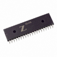
Z8523008PSG Zilog, Z8523008PSG Datasheet - Page 29

Z8523008PSG
Manufacturer Part Number
Z8523008PSG
Description
IC 8MHZ ESCC 40-DIP
Manufacturer
Zilog
Datasheet
1.Z8523008PSG.pdf
(117 pages)
Specifications of Z8523008PSG
Controller Type
Serial Communications Controller (SCC)
Interface
Bus
Voltage - Supply
4.5 V ~ 5.5 V
Current - Supply
4mA
Operating Temperature
0°C ~ 70°C
Mounting Type
Through Hole
Package / Case
40-DIP (0.620", 15.75mm)
Operating Supply Voltage
5 V
Supply Current (max)
9 mA
Maximum Operating Temperature
+ 70 C
Minimum Operating Temperature
0 C
Mounting Style
Through Hole
Lead Free Status / RoHS Status
Lead free / RoHS Compliant
Other names
269-3917
Z8523008PSG
Z8523008PSG
Available stocks
Company
Part Number
Manufacturer
Quantity
Price
Company:
Part Number:
Z8523008PSG
Manufacturer:
Zilog
Quantity:
177
PS005303-0907
WR7’ is written by first setting Bit 0 of Write Register 15 (WR15 bit 0) to 1 and then
accessing WR7. All write commands to register 7 are to WR7’ while WR15 bit 0 is set to
1. WR15 bit 0 must be reset to 0 to address the SYNC character in register WR7. If bit 6 of
WR7’ is set to 1, then WR7’ can be read by performing a read cycle to RR14. The WR7’
features remain enabled until specifically disabled or by a hardware or software reset. Bit
5 is set to 1 and all other bits are reset to 0 after a reset.
For applications which use either the Zilog Z8X30SCC or Z80230, these two device types
can be identified in software with the following test:
1. Write
2. Read Register 15
If bit 0 is set to 0, the device is Z8X30SCC. If bit 0 is set to 1, it is a Z80C30. If the device
is Z8XC30, a write to WR15 is required before proceeding. If the device is Z80230, all
writes to address 7 are to WR7’ until WR15 is set to 0.
The WR7 register bits are described below:
Bit 7 (Not used)
This bit must always be 0.
Bit 6 (Extended Read Enable)
Setting this bit to 1 enables WR3, WR4, WR5, WR7’ and WR10 to be read by issuing a
READ command for RR9 (WR3) RR4, RR5, RR14 (WR7’) and RR11 (WR10), respec-
tively.
Bit 5 (Transmit FIFO Interrupt Level)
If this bit is set to 1, the TBE interrupt is generated when the transmit FIFO is completely
empty. If this bit is set to 0, the TBE interrupt is generated when the top byte of the trans-
mit FIFO is empty. This bit is set following a hardware or channel reset.
In DMA REQUEST ON TRANSMIT mode, when using either the W/REQ or DTR/REQ
pins, the request is asserted when the Tx FIFO is completely empty if WR7’ bit 5 is set to
1. The request is asserted when the top byte of the FIFO is empty if bit 5 is reset.
Bit 4 (DTR/REQ Timing)
If this bit is set to 1 and the DTR/REQ pin is used for REQUEST mode (WR14 bit 2 is 1),
the deactivation of the DTR/REQ pin is identical to the W/REQ pin as illustrated in
Figure 12
01H
on page 25. If this bit is reset, the deactivation time is 4TcPc.
to Write Register 15
Z80230/Z85230 Enhancements
Product Specification
Z85230/Z80230
24


