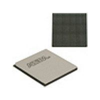
EP4SGX530HH35C2N Altera, EP4SGX530HH35C2N Datasheet - Page 537

EP4SGX530HH35C2N
Manufacturer Part Number
EP4SGX530HH35C2N
Description
IC STRATIX IV FPGA 530K 1152HBGA
Manufacturer
Altera
Series
Stratix® IV GXr
Datasheets
1.EP4SGX110DF29C3N.pdf
(80 pages)
2.EP4SGX110DF29C3N.pdf
(1154 pages)
3.EP4SGX110DF29C3N.pdf
(432 pages)
4.EP4SGX110DF29C3N.pdf
(22 pages)
5.EP4SGX110DF29C3N.pdf
(30 pages)
6.EP4SGX110DF29C3N.pdf
(72 pages)
7.EP4SGX530HH35C2N.pdf
(1145 pages)
Specifications of EP4SGX530HH35C2N
Number Of Logic Elements/cells
531200
Number Of Labs/clbs
21248
Total Ram Bits
27376
Number Of I /o
564
Voltage - Supply
0.87 V ~ 0.93 V
Mounting Type
Surface Mount
Operating Temperature
0°C ~ 85°C
Package / Case
1152-HBGA
Family Name
Stratix® IV
Number Of Logic Blocks/elements
531200
# Registers
424960
# I/os (max)
560
Process Technology
40nm
Operating Supply Voltage (typ)
900mV
Logic Cells
531200
Ram Bits
28033024
Operating Supply Voltage (min)
0.87V
Operating Supply Voltage (max)
0.93V
Operating Temp Range
0C to 85C
Operating Temperature Classification
Commercial
Mounting
Surface Mount
Pin Count
1152
Package Type
FCHBGA
Lead Free Status / RoHS Status
Lead free / RoHS Compliant
Number Of Gates
-
Lead Free Status / Rohs Status
Compliant
Available stocks
Company
Part Number
Manufacturer
Quantity
Price
- EP4SGX110DF29C3N PDF datasheet
- EP4SGX110DF29C3N PDF datasheet #2
- EP4SGX110DF29C3N PDF datasheet #3
- EP4SGX110DF29C3N PDF datasheet #4
- EP4SGX110DF29C3N PDF datasheet #5
- EP4SGX110DF29C3N PDF datasheet #6
- EP4SGX530HH35C2N PDF datasheet #7
- Current page: 537 of 1145
- Download datasheet (29Mb)
Chapter 1: Stratix IV Transceiver Architecture
Transceiver Block Architecture
Figure 1–85. CMU0 PLL
Note to
(1) The inter transceiver block (ITB) clock lines are the maximum value. The actual number of ITB lines in your device depends on the number of
© March 2010 Altera Corporation
transceiver blocks on one side of your device.
ITB Clock Lines (1)
PLL Cascade Clock
Figure
Global Clock Line
Dedicated refclk0
Dedicated refclk1
1–85:
f
f
1
6
CMU0 PLL
Figure 1–85
You can select the input reference clock to the CMU0 PLL from multiple clock sources:
■
■
■
■
■
The CMU0 PLL generates the high-speed clock from the input reference clock. The PFD
tracks the VCO output with the input reference clock.
For more information about transceiver input reference clocks, refer to the
Transceiver Clocking
The VCO in the CMU0 PLL is half rate and runs at half the serial data rate. To generate
the high-speed clock required to support a native data rate range of 600 Mbps to
8.5 Gbps, the CMU0 PLL uses two multiplier blocks (/M and /L) in the feedback path
(shown in
The ALTGX MegaWizard Plug-In Manager provides the list of input reference clock
frequencies based on the data rate you select. The Quartus II software automatically
selects the /M and /L settings based on the input reference clock frequency and serial
data rate.
The CMU0 and CMU1 PLLs have a dedicated pll_locked signal that is asserted to
indicate that the CMU PLL is locked to the input reference clock. You can use the
pll_locked signal in your transceiver reset sequence, as described in the
Control and Power Down
PLL cascade clock—the output from the general purpose PLLs in the FPGA fabric
Global clock line—the input reference clock from the dedicated CLK pins are
connected to the global clock line
refclk0—dedicated REFCLK in the transceiver block
refclk1—dedicated REFCLK in the transceiver block
Inter transceiver block lines—the ITB lines connect refclk0 and refclk1 of all
other transceiver blocks on the same side of the device
Input Reference
CMU0 PLL
Clock
Figure
/1, /2, /4, /8
shows the CMU0 PLL.
1–85).
chapter.
PFD
chapter.
CMU0 PLL
Charge Pump
+ Loop Filter
/M
V
CO
Stratix IV Device Handbook Volume 2
/L
High-Speed
Stratix IV
Reset
CMU0
Clock
1–99
Related parts for EP4SGX530HH35C2N
Image
Part Number
Description
Manufacturer
Datasheet
Request
R

Part Number:
Description:
CYCLONE II STARTER KIT EP2C20N
Manufacturer:
Altera
Datasheet:

Part Number:
Description:
CPLD, EP610 Family, ECMOS Process, 300 Gates, 16 Macro Cells, 16 Reg., 16 User I/Os, 5V Supply, 35 Speed Grade, 24DIP
Manufacturer:
Altera Corporation
Datasheet:

Part Number:
Description:
CPLD, EP610 Family, ECMOS Process, 300 Gates, 16 Macro Cells, 16 Reg., 16 User I/Os, 5V Supply, 15 Speed Grade, 24DIP
Manufacturer:
Altera Corporation
Datasheet:

Part Number:
Description:
Manufacturer:
Altera Corporation
Datasheet:

Part Number:
Description:
CPLD, EP610 Family, ECMOS Process, 300 Gates, 16 Macro Cells, 16 Reg., 16 User I/Os, 5V Supply, 30 Speed Grade, 24DIP
Manufacturer:
Altera Corporation
Datasheet:

Part Number:
Description:
High-performance, low-power erasable programmable logic devices with 8 macrocells, 10ns
Manufacturer:
Altera Corporation
Datasheet:

Part Number:
Description:
High-performance, low-power erasable programmable logic devices with 8 macrocells, 7ns
Manufacturer:
Altera Corporation
Datasheet:

Part Number:
Description:
Classic EPLD
Manufacturer:
Altera Corporation
Datasheet:

Part Number:
Description:
High-performance, low-power erasable programmable logic devices with 8 macrocells, 10ns
Manufacturer:
Altera Corporation
Datasheet:

Part Number:
Description:
Manufacturer:
Altera Corporation
Datasheet:

Part Number:
Description:
Manufacturer:
Altera Corporation
Datasheet:

Part Number:
Description:
Manufacturer:
Altera Corporation
Datasheet:

Part Number:
Description:
CPLD, EP610 Family, ECMOS Process, 300 Gates, 16 Macro Cells, 16 Reg., 16 User I/Os, 5V Supply, 25 Speed Grade, 24DIP
Manufacturer:
Altera Corporation
Datasheet:


