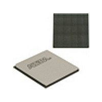
EP4SGX530HH35C2N Altera, EP4SGX530HH35C2N Datasheet - Page 302

EP4SGX530HH35C2N
Manufacturer Part Number
EP4SGX530HH35C2N
Description
IC STRATIX IV FPGA 530K 1152HBGA
Manufacturer
Altera
Series
Stratix® IV GXr
Datasheets
1.EP4SGX110DF29C3N.pdf
(80 pages)
2.EP4SGX110DF29C3N.pdf
(1154 pages)
3.EP4SGX110DF29C3N.pdf
(432 pages)
4.EP4SGX110DF29C3N.pdf
(22 pages)
5.EP4SGX110DF29C3N.pdf
(30 pages)
6.EP4SGX110DF29C3N.pdf
(72 pages)
7.EP4SGX530HH35C2N.pdf
(1145 pages)
Specifications of EP4SGX530HH35C2N
Number Of Logic Elements/cells
531200
Number Of Labs/clbs
21248
Total Ram Bits
27376
Number Of I /o
564
Voltage - Supply
0.87 V ~ 0.93 V
Mounting Type
Surface Mount
Operating Temperature
0°C ~ 85°C
Package / Case
1152-HBGA
Family Name
Stratix® IV
Number Of Logic Blocks/elements
531200
# Registers
424960
# I/os (max)
560
Process Technology
40nm
Operating Supply Voltage (typ)
900mV
Logic Cells
531200
Ram Bits
28033024
Operating Supply Voltage (min)
0.87V
Operating Supply Voltage (max)
0.93V
Operating Temp Range
0C to 85C
Operating Temperature Classification
Commercial
Mounting
Surface Mount
Pin Count
1152
Package Type
FCHBGA
Lead Free Status / RoHS Status
Lead free / RoHS Compliant
Number Of Gates
-
Lead Free Status / Rohs Status
Compliant
Available stocks
Company
Part Number
Manufacturer
Quantity
Price
- EP4SGX110DF29C3N PDF datasheet
- EP4SGX110DF29C3N PDF datasheet #2
- EP4SGX110DF29C3N PDF datasheet #3
- EP4SGX110DF29C3N PDF datasheet #4
- EP4SGX110DF29C3N PDF datasheet #5
- EP4SGX110DF29C3N PDF datasheet #6
- EP4SGX530HH35C2N PDF datasheet #7
- Current page: 302 of 1145
- Download datasheet (29Mb)
8–22
Receiver Data Path Modes
Figure 8–18. Receiver Data Path in Non-DPA Mode
Notes to
(1) In SDR and DDR modes, the data width from the IOE is 1 and 2 bits, respectively.
(2) The rx_out port has a maximum data width of 10 bits.
Stratix IV Device Handbook Volume 1
rx_divfwdclk
rx_outclock
Fabric
FPGA
Figure
rx_out
8–18:
10
The Stratix IV device family supports three receiver datapath modes—non-DPA
mode, DPA mode, and soft-CDR mode.
Non-DPA Mode
Figure 8–18
and synchronizer blocks are disabled. Input serial data is registered at the rising or
falling edge of the serial LVDS_diffioclk clock produced by the left and right PLL.
You can select the rising/falling edge option using the ALTLDVS MegaWizard
Plug-In Manager software. Both data realignment and deserializer blocks are clocked
by the LVDS_diffioclk clock, which is generated by the left and right PLL.
IOE Supports SDR, DDR, or Non-Registered Datapath
(LOAD_EN, diffioclk)
2
Deserializer
DOUT DIN
shows the non-DPA datapath block diagram. In non-DPA mode, the DPA
IOE
2
Left/Right PLL
3
DOUT DIN
Clock Mux
(Note
Bit Slip
(LVDS_LOAD_EN,
LVDS_diffioclk,
Chapter 8: High-Speed Differential I/O Interfaces and DPA in Stratix IV Devices
rx_outclk)
diffioclk
1),
(2)
rx_inclock
8 Serial LVDS
Clock Phases
Synchronizer
DOUT DIN
L L
LVDS Receiver
N
3
(DPA_LO
DPA_diffioclk,
rx_divfwdclk)
P P
P P
© March 2010 Altera Corporation
AD_EN,
DPA Circuitr
Retimed
DPA Cloc
LVDS Clock Domain
P P
P P
Data
k
Differential Receiver
DIN
y
+
rx_in
Related parts for EP4SGX530HH35C2N
Image
Part Number
Description
Manufacturer
Datasheet
Request
R

Part Number:
Description:
CYCLONE II STARTER KIT EP2C20N
Manufacturer:
Altera
Datasheet:

Part Number:
Description:
CPLD, EP610 Family, ECMOS Process, 300 Gates, 16 Macro Cells, 16 Reg., 16 User I/Os, 5V Supply, 35 Speed Grade, 24DIP
Manufacturer:
Altera Corporation
Datasheet:

Part Number:
Description:
CPLD, EP610 Family, ECMOS Process, 300 Gates, 16 Macro Cells, 16 Reg., 16 User I/Os, 5V Supply, 15 Speed Grade, 24DIP
Manufacturer:
Altera Corporation
Datasheet:

Part Number:
Description:
Manufacturer:
Altera Corporation
Datasheet:

Part Number:
Description:
CPLD, EP610 Family, ECMOS Process, 300 Gates, 16 Macro Cells, 16 Reg., 16 User I/Os, 5V Supply, 30 Speed Grade, 24DIP
Manufacturer:
Altera Corporation
Datasheet:

Part Number:
Description:
High-performance, low-power erasable programmable logic devices with 8 macrocells, 10ns
Manufacturer:
Altera Corporation
Datasheet:

Part Number:
Description:
High-performance, low-power erasable programmable logic devices with 8 macrocells, 7ns
Manufacturer:
Altera Corporation
Datasheet:

Part Number:
Description:
Classic EPLD
Manufacturer:
Altera Corporation
Datasheet:

Part Number:
Description:
High-performance, low-power erasable programmable logic devices with 8 macrocells, 10ns
Manufacturer:
Altera Corporation
Datasheet:

Part Number:
Description:
Manufacturer:
Altera Corporation
Datasheet:

Part Number:
Description:
Manufacturer:
Altera Corporation
Datasheet:

Part Number:
Description:
Manufacturer:
Altera Corporation
Datasheet:

Part Number:
Description:
CPLD, EP610 Family, ECMOS Process, 300 Gates, 16 Macro Cells, 16 Reg., 16 User I/Os, 5V Supply, 25 Speed Grade, 24DIP
Manufacturer:
Altera Corporation
Datasheet:


