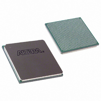
EP1S20F780I6N Altera, EP1S20F780I6N Datasheet - Page 722

EP1S20F780I6N
Manufacturer Part Number
EP1S20F780I6N
Description
IC STRATIX FPGA 20K LE 780-FBGA
Manufacturer
Altera
Series
Stratix®r
Specifications of EP1S20F780I6N
Number Of Logic Elements/cells
18460
Number Of Labs/clbs
1846
Total Ram Bits
1669248
Number Of I /o
586
Voltage - Supply
1.425 V ~ 1.575 V
Mounting Type
Surface Mount
Operating Temperature
-40°C ~ 100°C
Package / Case
780-FBGA
Family Name
Stratix
Number Of Logic Blocks/elements
18460
# I/os (max)
586
Frequency (max)
450.05MHz
Process Technology
0.13um (CMOS)
Operating Supply Voltage (typ)
1.5V
Logic Cells
18460
Ram Bits
1669248
Operating Supply Voltage (min)
1.425V
Operating Supply Voltage (max)
1.575V
Operating Temp Range
-40C to 100C
Operating Temperature Classification
Industrial
Mounting
Surface Mount
Pin Count
780
Package Type
FC-FBGA
Lead Free Status / RoHS Status
Lead free / RoHS Compliant
Number Of Gates
-
Lead Free Status / Rohs Status
Compliant
Available stocks
Company
Part Number
Manufacturer
Quantity
Price
Company:
Part Number:
EP1S20F780I6N
Manufacturer:
ALTERA
Quantity:
3 000
- Current page: 722 of 864
- Download datasheet (11Mb)
Device Configuration Overview
11–4
Stratix Device Handbook, Volume 2
related I/O banks (3, 4, 7, and 8) where the following pins reside: TDI,
TMS, TCK, TRST, MSEL0, MSEL1, MSEL2, nCONFIG, nCE, DCLK, PLL_ENA,
CONF_DONE, nSTATUS. The VCCSEL pin can be pulled to 1.5, 1.8, 2.5, or
3.3-V for a logic high level. There is an internal 2.5-k pull-down resistor
on VCCSEL. Therefore, if you are using a pull-up resister to pull up this
signal, you need to use a 1-k resistor.
VCCSEL also sets the power-on-reset (POR) trip point for all the
configuration related I/O banks (3, 4, 7, and 8), ensuring that these I/O
banks have powered up to the appropriate voltage levels before
configuration begins. Upon power-up, the FPGA does not release
nSTATUS until V
banks are above their POR trip points. If you set VCCSEL to ground (logic
low), this sets the POR trip point for all configuration I/O banks to a
voltage consistent with 3.3-V/2.5-V signaling. When VCCSEL = 0, the
POR trip point for these I/O banks may be as high as 1.8 V. If V
of the configuration banks is set to 1.8 or 1.5 V, the voltage supplied to this
I/O bank(s) may never reach the POR trip point, which will not allow the
FPGA to begin configuration.
1
Table 11–3
V
input signaling voltages.
The VCCSEL signal does not control any of the dual-purpose pins,
including the dual-purpose configuration pins, such as the DATA[7..0]
and PPA pins (nWS, nRS, CS, nCS, and RDYnBSY). During configuration,
these dual-purpose pins drive out voltage levels corresponding to the
V
configuration, the dual-purpose pins inherit the I/O standards specified
in the design.
3.3-V/2.5-V
1.8-V/1.5-V
3.3-V/2.5-V
Table 11–3. VCCSEL Setting
CCIO
CCIO
V
CCIO
setting of the configuration I/O banks and your configuration
supply voltage that powers the I/O bank containing the pin. After
(banks 3,4,7,8)
If the V
configuration signals used require 3.3-V or 2.5-V signaling you
should set VCCSEL to V
trip point to enable successful configuration.
shows how you should set the VCCSEL depending on the
CCIO
CCINT
of I/O banks 3, 4, 7, or 8 is set to 1.5 or 1.8 V and the
and all of the V
3.3-V/2.5-V
3.3-V/2.5-V/1.8-V/1.5-V
1.8-V/1.5-V
Configuration Input
Signaling Voltage
CC
(logic high) in order to lower the POR
CCIO
s of the configuration I/O
GND
VCC
Not Supported
Altera Corporation
V
CCSEL
CCIO
July 2005
of any
Related parts for EP1S20F780I6N
Image
Part Number
Description
Manufacturer
Datasheet
Request
R

Part Number:
Description:
CYCLONE II STARTER KIT EP2C20N
Manufacturer:
Altera
Datasheet:

Part Number:
Description:
CPLD, EP610 Family, ECMOS Process, 300 Gates, 16 Macro Cells, 16 Reg., 16 User I/Os, 5V Supply, 35 Speed Grade, 24DIP
Manufacturer:
Altera Corporation
Datasheet:

Part Number:
Description:
CPLD, EP610 Family, ECMOS Process, 300 Gates, 16 Macro Cells, 16 Reg., 16 User I/Os, 5V Supply, 15 Speed Grade, 24DIP
Manufacturer:
Altera Corporation
Datasheet:

Part Number:
Description:
Manufacturer:
Altera Corporation
Datasheet:

Part Number:
Description:
CPLD, EP610 Family, ECMOS Process, 300 Gates, 16 Macro Cells, 16 Reg., 16 User I/Os, 5V Supply, 30 Speed Grade, 24DIP
Manufacturer:
Altera Corporation
Datasheet:

Part Number:
Description:
High-performance, low-power erasable programmable logic devices with 8 macrocells, 10ns
Manufacturer:
Altera Corporation
Datasheet:

Part Number:
Description:
High-performance, low-power erasable programmable logic devices with 8 macrocells, 7ns
Manufacturer:
Altera Corporation
Datasheet:

Part Number:
Description:
Classic EPLD
Manufacturer:
Altera Corporation
Datasheet:

Part Number:
Description:
High-performance, low-power erasable programmable logic devices with 8 macrocells, 10ns
Manufacturer:
Altera Corporation
Datasheet:

Part Number:
Description:
Manufacturer:
Altera Corporation
Datasheet:

Part Number:
Description:
Manufacturer:
Altera Corporation
Datasheet:

Part Number:
Description:
Manufacturer:
Altera Corporation
Datasheet:

Part Number:
Description:
CPLD, EP610 Family, ECMOS Process, 300 Gates, 16 Macro Cells, 16 Reg., 16 User I/Os, 5V Supply, 25 Speed Grade, 24DIP
Manufacturer:
Altera Corporation
Datasheet:


