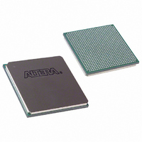
EP1S20F780I6N Altera, EP1S20F780I6N Datasheet - Page 381

EP1S20F780I6N
Manufacturer Part Number
EP1S20F780I6N
Description
IC STRATIX FPGA 20K LE 780-FBGA
Manufacturer
Altera
Series
Stratix®r
Specifications of EP1S20F780I6N
Number Of Logic Elements/cells
18460
Number Of Labs/clbs
1846
Total Ram Bits
1669248
Number Of I /o
586
Voltage - Supply
1.425 V ~ 1.575 V
Mounting Type
Surface Mount
Operating Temperature
-40°C ~ 100°C
Package / Case
780-FBGA
Family Name
Stratix
Number Of Logic Blocks/elements
18460
# I/os (max)
586
Frequency (max)
450.05MHz
Process Technology
0.13um (CMOS)
Operating Supply Voltage (typ)
1.5V
Logic Cells
18460
Ram Bits
1669248
Operating Supply Voltage (min)
1.425V
Operating Supply Voltage (max)
1.575V
Operating Temp Range
-40C to 100C
Operating Temperature Classification
Industrial
Mounting
Surface Mount
Pin Count
780
Package Type
FC-FBGA
Lead Free Status / RoHS Status
Lead free / RoHS Compliant
Number Of Gates
-
Lead Free Status / Rohs Status
Compliant
Available stocks
Company
Part Number
Manufacturer
Quantity
Price
Company:
Part Number:
EP1S20F780I6N
Manufacturer:
ALTERA
Quantity:
3 000
- Current page: 381 of 864
- Download datasheet (11Mb)
Altera Corporation
July 2005
f
In true dual-port configuration, the RAM outputs can only be configured
for read-during-write mode. This means that during write operation,
data being written to the A or B port of the RAM flows through to the A
or B outputs, respectively. When the output registers are bypassed, the
new data is available on the rising edge of the same clock cycle it was
written on. For waveforms and information on mixed-port read-during-
write mode, see
page
Potential write contentions must be resolved external to the RAM because
writing to the same address location at both ports results in unknown
data storage at that location. Data is written on the rising edge of the write
clock for the M-RAM block. For a valid write operation to the same
address of the M-RAM block, the rising edge of the write clock for port A
must occur following the maximum write cycle time interval after the
rising edge of the write clock for port B. Since data is written into the
M512 and M4K blocks at the falling edge of the write clock, the rising
edge of the write clock for port A should occur following half of the
maximum write cycle time interval after the falling edge of the write clock
for port B. If this timing is not met, the data stored in that particular
address is invalid.
See the Stratix Device Family Data Sheet section of the Stratix Device
Handbook, Volume 1 or the Stratix GX Device Family Data Sheet section of
the Stratix GX Device Handbook, Volume 1 for the maximum synchronous
write cycle time.
Figure 2–7
port A and read operation at port B.
Table 2–11. M-RAM Block Mixed-Port Width Configurations (True Dual-Port)
2–25.
32K
16K
64K
8K
TriMatrix Embedded Memory Blocks in Stratix & Stratix GX Devices
Port A
shows true dual-port timing waveforms for write operation at
72
18
36
9
“Read-During-Write Operation at the Same Address” on
64K
v
v
v
v
9
32K
Stratix Device Handbook, Volume 2
v
v
v
v
18
Port B
16K
v
v
v
v
36
8K
v
v
v
v
72
2–13
Related parts for EP1S20F780I6N
Image
Part Number
Description
Manufacturer
Datasheet
Request
R

Part Number:
Description:
CYCLONE II STARTER KIT EP2C20N
Manufacturer:
Altera
Datasheet:

Part Number:
Description:
CPLD, EP610 Family, ECMOS Process, 300 Gates, 16 Macro Cells, 16 Reg., 16 User I/Os, 5V Supply, 35 Speed Grade, 24DIP
Manufacturer:
Altera Corporation
Datasheet:

Part Number:
Description:
CPLD, EP610 Family, ECMOS Process, 300 Gates, 16 Macro Cells, 16 Reg., 16 User I/Os, 5V Supply, 15 Speed Grade, 24DIP
Manufacturer:
Altera Corporation
Datasheet:

Part Number:
Description:
Manufacturer:
Altera Corporation
Datasheet:

Part Number:
Description:
CPLD, EP610 Family, ECMOS Process, 300 Gates, 16 Macro Cells, 16 Reg., 16 User I/Os, 5V Supply, 30 Speed Grade, 24DIP
Manufacturer:
Altera Corporation
Datasheet:

Part Number:
Description:
High-performance, low-power erasable programmable logic devices with 8 macrocells, 10ns
Manufacturer:
Altera Corporation
Datasheet:

Part Number:
Description:
High-performance, low-power erasable programmable logic devices with 8 macrocells, 7ns
Manufacturer:
Altera Corporation
Datasheet:

Part Number:
Description:
Classic EPLD
Manufacturer:
Altera Corporation
Datasheet:

Part Number:
Description:
High-performance, low-power erasable programmable logic devices with 8 macrocells, 10ns
Manufacturer:
Altera Corporation
Datasheet:

Part Number:
Description:
Manufacturer:
Altera Corporation
Datasheet:

Part Number:
Description:
Manufacturer:
Altera Corporation
Datasheet:

Part Number:
Description:
Manufacturer:
Altera Corporation
Datasheet:

Part Number:
Description:
CPLD, EP610 Family, ECMOS Process, 300 Gates, 16 Macro Cells, 16 Reg., 16 User I/Os, 5V Supply, 25 Speed Grade, 24DIP
Manufacturer:
Altera Corporation
Datasheet:


