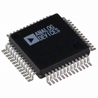
ADUC836BSZ Analog Devices Inc, ADUC836BSZ Datasheet - Page 8

ADUC836BSZ
Manufacturer Part Number
ADUC836BSZ
Description
16bit Dual ADC With Embedded 8 Bit MCU
Manufacturer
Analog Devices Inc
Series
MicroConverter® ADuC8xxr
Datasheet
1.ADUC836BSZ.pdf
(80 pages)
Specifications of ADUC836BSZ
Core Processor
8052
Core Size
8-Bit
Speed
12.58MHz
Connectivity
EBI/EMI, I²C, SPI, UART/USART
Peripherals
POR, PSM, PWM, Temp Sensor, WDT
Number Of I /o
34
Program Memory Size
62KB (62K x 8)
Program Memory Type
FLASH
Eeprom Size
4K x 8
Ram Size
2.25K x 8
Voltage - Supply (vcc/vdd)
2.7 V ~ 5.25 V
Data Converters
A/D 7x16b; D/A 1x12b
Oscillator Type
Internal
Operating Temperature
-40°C ~ 125°C
Package / Case
52-MQFP, 52-PQFP
Cpu Family
ADuC8xx
Device Core
8052
Device Core Size
8b
Frequency (max)
12.58MHz
Interface Type
I2C/SPI/UART
Total Internal Ram Size
2.25KB
# I/os (max)
26
Number Of Timers - General Purpose
3
Operating Supply Voltage (typ)
3.3/5V
Operating Supply Voltage (max)
5.25V
Operating Supply Voltage (min)
2.7V
On-chip Adc
2(2-chx16-bit)
On-chip Dac
1-chx12-bit
Instruction Set Architecture
CISC
Operating Temp Range
-40C to 125C
Operating Temperature Classification
Automotive
Mounting
Surface Mount
Pin Count
52
Package Type
MQFP
Package
52MQFP
Family Name
ADuC8xx
Maximum Speed
12.58 MHz
Operating Supply Voltage
3.3|5 V
Data Bus Width
8 Bit
Number Of Programmable I/os
26
Number Of Timers
3
Lead Free Status / RoHS Status
Lead free / RoHS Compliant
Lead Free Status / RoHS Status
Lead free / RoHS Compliant
Available stocks
Company
Part Number
Manufacturer
Quantity
Price
Company:
Part Number:
ADUC836BSZ
Manufacturer:
ADI
Quantity:
150
Company:
Part Number:
ADUC836BSZ
Manufacturer:
Analog Devices Inc
Quantity:
10 000
Part Number:
ADUC836BSZ
Manufacturer:
ADI/亚德诺
Quantity:
20 000
ADuC836
NOTES
10
11
12
13
14
15
16
17
18
19
Specifications subject to change without notice.
1
2
3
4
5
6
7
8
9
Temperature range for ADuC836BS (MQFP package) is –40°C to +125°C. Temperature range for ADuC836BCP (CSP package) is –40°C to +85°C.
These numbers are not production tested but are guaranteed by design and/or characterization data on production release.
The primary ADC is factory calibrated at 25°C with AV
The auxiliary ADC is factory calibrated at 25°C with AV
System Zero-Scale Calibration can remove this error.
different from these, an Internal Full-Scale Calibration will restore this error to 10 V. A system zero-scale and full-scale calibration will remove this error altogether.
Gain Error Drift is a span drift. To calculate Full-Scale Error Drift, add the Offset Error Drift to the Gain Error Drift times the full-scale input.
will remove this error altogether.
DAC linearity and ac specifications are calculated using: reduced code range of 48 to 4095, 0 to V
Gain Error is a measurement of the span error of the DAC.
In general terms, the bipolar input voltage range to the primary ADC is given by Range
V
V
1.25 V is used as the reference voltage to the auxiliary ADC when internal V
In Bipolar mode, the auxiliary ADC can only be driven to a minimum of AGND – 30 mV as indicated by the auxiliary ADC absolute AIN voltage limits. The bipolar
range is still –V
The ADuC836BCP (CSP package) has been qualified and tested with the base of the CSP package floating.
Pins configured in SPI mode, pins configured as digital inputs during this test.
Pins configured in I
Flash/EE Memory Reliability Characteristics apply to both the Flash/EE program memory and Flash/EE data memory.
Endurance is qualified to 100 Kcycles as per JEDEC Std. 22 method A117 and measured at –40°C, +25°C, +85°C, and +125°C.Typical endurance at 25°C is 700 Kcycles.
Retention lifetime equivalent at junction temperature (T
derate with junction temperature as shown in Figure 16 in the Flash/EE Memory section.
Power Supply current consumption is measured in Normal, Idle, and Power-Down modes under the following conditions:
Normal mode: Reset = 0.4 V, Digital I/O pins = open circuit, Core Clk changed via CD bits in PLLCON, Core Executing internal software loop.
Idle mode: Reset = 0.4 V, Digital I/O pins = open circuit, Core Clk changed via CD bits in PLLCON, PCON.0 = 1, Core Execution suspended in idle mode.
Power-Down mode: Reset = 0.4 V, All P0 pins and P1.2–P1.7 pins = 0.4 V, all other digital I/O pins are open circuit, Core Clk changed via CD bits in PLLCON,
PCON.1 = 1, Core Execution suspended in Power-Down mode, OSC turned on or off via OSC_PD bit (PLLCON.7) in PLLCON SFR.
DV
REF
REF
DD
= REFIN(+) to REFIN(–) voltage and V
= 2.5 V and RN2, RN1, RN0 = 1, 1, 0 the Range
power supply current will increase typically by 3 mA (3 V operation) and 10 mA (5 V operation) during a Flash/EE memory program or erase cycle.
REF
to +V
2
C mode only.
REF
; however, the negative voltage is limited to –30 mV.
REF
= 1.25 V when internal ADC V
DD
ADC
= DV
DD
J
) = 55°C as per JEDEC Std. 22, Method A117. Retention lifetime based on an activation energy of 0.6 eV will
= ±1.28 V. In Unipolar mode, the effective range is 0 V to 1.28 V in our example.
= DV
DD
= 5 V yielding this full-scale error of 10 V. If user power supply or temperature conditions are significantly
DD
= 5 V yielding this full-scale error of –2.5 LSB. A system zero-scale and full-scale calibration
REF
is selected via XREF0 and XREF1 bits in ADC0CON and ADC1CON, respectively.
REF
–8–
is selected. RN = decimal equivalent of RN2, RN1, RN0, e.g.,
ADC
= ±(V
REF
REF
; reduced code range of 100 to 3950, 0 to V
2
RN
)/125, where:
DD
.
REV. A


