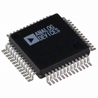
ADUC836BSZ Analog Devices Inc, ADUC836BSZ Datasheet - Page 30

ADUC836BSZ
Manufacturer Part Number
ADUC836BSZ
Description
16bit Dual ADC With Embedded 8 Bit MCU
Manufacturer
Analog Devices Inc
Series
MicroConverter® ADuC8xxr
Datasheet
1.ADUC836BSZ.pdf
(80 pages)
Specifications of ADUC836BSZ
Core Processor
8052
Core Size
8-Bit
Speed
12.58MHz
Connectivity
EBI/EMI, I²C, SPI, UART/USART
Peripherals
POR, PSM, PWM, Temp Sensor, WDT
Number Of I /o
34
Program Memory Size
62KB (62K x 8)
Program Memory Type
FLASH
Eeprom Size
4K x 8
Ram Size
2.25K x 8
Voltage - Supply (vcc/vdd)
2.7 V ~ 5.25 V
Data Converters
A/D 7x16b; D/A 1x12b
Oscillator Type
Internal
Operating Temperature
-40°C ~ 125°C
Package / Case
52-MQFP, 52-PQFP
Cpu Family
ADuC8xx
Device Core
8052
Device Core Size
8b
Frequency (max)
12.58MHz
Interface Type
I2C/SPI/UART
Total Internal Ram Size
2.25KB
# I/os (max)
26
Number Of Timers - General Purpose
3
Operating Supply Voltage (typ)
3.3/5V
Operating Supply Voltage (max)
5.25V
Operating Supply Voltage (min)
2.7V
On-chip Adc
2(2-chx16-bit)
On-chip Dac
1-chx12-bit
Instruction Set Architecture
CISC
Operating Temp Range
-40C to 125C
Operating Temperature Classification
Automotive
Mounting
Surface Mount
Pin Count
52
Package Type
MQFP
Package
52MQFP
Family Name
ADuC8xx
Maximum Speed
12.58 MHz
Operating Supply Voltage
3.3|5 V
Data Bus Width
8 Bit
Number Of Programmable I/os
26
Number Of Timers
3
Lead Free Status / RoHS Status
Lead free / RoHS Compliant
Lead Free Status / RoHS Status
Lead free / RoHS Compliant
Available stocks
Company
Part Number
Manufacturer
Quantity
Price
Company:
Part Number:
ADUC836BSZ
Manufacturer:
ADI
Quantity:
150
Company:
Part Number:
ADUC836BSZ
Manufacturer:
Analog Devices Inc
Quantity:
10 000
Part Number:
ADUC836BSZ
Manufacturer:
ADI/亚德诺
Quantity:
20 000
Flash/EE Program Memory
The ADuC836 contains a 64 Kbyte array of Flash/EE program
memory. The lower 62 Kbytes of this program memory are avail-
able to the user, and can be used for program storage or indeed
as additional NV data memory.
The upper 2 Kbytes of this Flash/EE program memory array con-
tain permanently embedded firmware, allowing in-circuit serial
download, serial debug, and nonintrusive single pin emulation.
These 2 Kbytes of embedded firmware also contain a power-on
configuration routine that downloads factory calibrated coeffi-
cients to the various calibrated peripherals (ADC, temperature
sensor, current sources, band gap references, and so on).
This 2 Kbyte embedded firmware is hidden from user code.
Attempts to read this space will read 0s, i.e., the embedded firm-
ware appears as NOP instructions to user code.
In normal operating mode (power-up default), the 62 Kbytes of
user Flash/EE program memory appear as a single block. This
block is used to store the user code, as shown in Figure 17.
In Normal mode, the 62 Kbytes of Flash/EE program memory
can be programmed by serial downloading or parallel processing:
(1) Serial Downloading (In-Circuit Programming)
The ADuC836 facilitates code download via the standard UART
serial port.The ADuC836 will enter Serial Download mode after
a reset or power cycle if the PSEN pin is pulled low through an
external 1 k resistor. Once in serial download mode, the hidden
embedded download kernel will execute.This allows the user to
download code to the full 62 Kbytes of Flash/EE program memo-
ry while the device is in circuit in its target application hardware.
A PC serial download executable is provided as part of the
ADuC836 QuickStart development system. Application Note
uC004 fully describes the serial download protocol that is used
by the embedded download kernel. This Application Note is
available at www.analog.com/microconverter.
ADuC836
Figure 17 . Flash/EE Program Memory Map in Normal Mode
PERMANENTLY EMBEDDED FIRMWARE ALLOWS CODE
ON-CHIP PROGRAM MEMORY. THE KERNEL PROGRAM
TO BE DOWNLOADED TO ANY OF THE 62 KBYTES OF
AVAILABLE TO THE USER. ALL OF THIS SPACE CAN
APPEARS AS ‘NOP’ INSTRUCTIONS TO USER CODE.
62 KBYTES OF FLASH/EE PROGRAM MEMORY IS
EMBEDDED DOWNLOAD/DEBUG KERNEL OR IN
BE PROGRAMMED FROM THE PERMANENTLY
EMBEDDED DOWNLOAD/DEBUG KERNEL
PARALLEL PROGRAMMING MODE.
USER PROGRAM MEMORY
62 KBYTE
2 KBYTE
FFFFH
F800H
F7FFH
0000H
–30–
(2) Parallel Programming
The Parallel Programming mode is fully compatible with con-
ventional third party Flash or EEPROM device programmers.
A block diagram of the external pin configuration required to
support parallel programming is shown in Figure 18. In this mode,
Ports 0 and 2 operate as the external address bus interface, P3
operates as the external data bus interface, and P1.0 operates as
the Write Enable strobe. Port 1.1, P1.2, P1.3, and P1.4 are used
as a general configuration port that configures the device for vari-
ous program and erase operations during parallel programming.
P1.4
0
1
1
0
1
0
1
1
All other codes
Table XIII. Flash/EE Memory Parallel Programming Modes
SEQUENCE
PROGRAM MODE
(SEE TABLE XIII)
Figure 18. Flash/EE Memory Parallel Programming
ENTRY
Port 1 Pins
P1.3
0
0
0
0
0
0
1
1
COMMAND
ENABLE
GND
GND
V
DD
P1.2
0
0
1
1
1
1
0
0
5V
P1.1
0
1
0
0
1
1
0
1
P1.1 -> P1.4
P1.0
EA
PSEN
RESET
V
GND
DD
ADuC836
Programming Mode
Erase Flash/EE Program,
Data, and Security Modes
Read Device Signature/ID
Program Code Byte
Program Data Byte
Read Code Byte
Read Data Byte
Program Security Modes
Read/Verify Security Modes
Redundant
P1.5 -> P1.7
P0
P3
P2
PROGRAM
DATA
(D0–D7)
PROGRAM
ADDRESS
(A0–A13)
(P2.0 = A0)
(P1.7 = A13)
TIMING
REV. A


