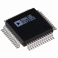
ADUC836BSZ Analog Devices Inc, ADUC836BSZ Datasheet - Page 63

ADUC836BSZ
Manufacturer Part Number
ADUC836BSZ
Description
16bit Dual ADC With Embedded 8 Bit MCU
Manufacturer
Analog Devices Inc
Series
MicroConverter® ADuC8xxr
Datasheet
1.ADUC836BSZ.pdf
(80 pages)
Specifications of ADUC836BSZ
Core Processor
8052
Core Size
8-Bit
Speed
12.58MHz
Connectivity
EBI/EMI, I²C, SPI, UART/USART
Peripherals
POR, PSM, PWM, Temp Sensor, WDT
Number Of I /o
34
Program Memory Size
62KB (62K x 8)
Program Memory Type
FLASH
Eeprom Size
4K x 8
Ram Size
2.25K x 8
Voltage - Supply (vcc/vdd)
2.7 V ~ 5.25 V
Data Converters
A/D 7x16b; D/A 1x12b
Oscillator Type
Internal
Operating Temperature
-40°C ~ 125°C
Package / Case
52-MQFP, 52-PQFP
Cpu Family
ADuC8xx
Device Core
8052
Device Core Size
8b
Frequency (max)
12.58MHz
Interface Type
I2C/SPI/UART
Total Internal Ram Size
2.25KB
# I/os (max)
26
Number Of Timers - General Purpose
3
Operating Supply Voltage (typ)
3.3/5V
Operating Supply Voltage (max)
5.25V
Operating Supply Voltage (min)
2.7V
On-chip Adc
2(2-chx16-bit)
On-chip Dac
1-chx12-bit
Instruction Set Architecture
CISC
Operating Temp Range
-40C to 125C
Operating Temperature Classification
Automotive
Mounting
Surface Mount
Pin Count
52
Package Type
MQFP
Package
52MQFP
Family Name
ADuC8xx
Maximum Speed
12.58 MHz
Operating Supply Voltage
3.3|5 V
Data Bus Width
8 Bit
Number Of Programmable I/os
26
Number Of Timers
3
Lead Free Status / RoHS Status
Lead free / RoHS Compliant
Lead Free Status / RoHS Status
Lead free / RoHS Compliant
Available stocks
Company
Part Number
Manufacturer
Quantity
Price
Company:
Part Number:
ADUC836BSZ
Manufacturer:
ADI
Quantity:
150
Company:
Part Number:
ADUC836BSZ
Manufacturer:
Analog Devices Inc
Quantity:
10 000
Part Number:
ADUC836BSZ
Manufacturer:
ADI/亚德诺
Quantity:
20 000
ADuC836 HARDWARE DESIGN CONSIDERATIONS
This section outlines some of the key hardware design consider-
ations that must be addressed when integrating the ADuC836
into any hardware system.
External Memory Interface
In addition to its internal program and data memories, the
ADuC836 can access up to 64 Kbytes of external program memory
(ROM, PROM, and so on) and up to 16 Mbytes of external data
memory (SRAM).
To select from which code space (internal or external program
memory) to begin executing code, tie the EA (external access)
pin high or low, respectively. When EA is high (pulled up to V
user program execution will start at Address 0 in the internal
62 Kbytes Flash/EE code space. When EA is low (tied to ground)
user program execution will start at Address 0 in the external
code space. When executing from internal code space, accesses
to the program space above F7FFH (62 Kbytes) will be read as
NOP instructions.
Note that a second very important function of the EA pin is
described in the Single Pin Emulation Mode section.
External program memory (if used) must be connected to the
ADuC836, as illustrated in Figure 58. Sixteen I/O lines (Ports 0
and 2) are dedicated to bus functions during external program
memory fetches. Port 0 (P0) serves as a multiplexed address/data
bus. It emits the low byte of the program counter (PCL) as
an address, and then goes into a high impedance input state
awaiting the arrival of the code byte from the program memory.
During the time that the low byte of the program counter is valid
on P0, the signal ALE (Address Latch Enable) clocks this byte
into an external address latch. Meanwhile, Port 2 (P2) emits the
high byte of the program counter (PCH), and PSEN strobes the
EPROM and the code byte is read into the ADuC836.
Note that program memory addresses are always 16 bits wide,
even in cases where the actual amount of program memory used
is less than 64 Kbytes. External program execution sacrifices
two of the 8-bit ports (P0 and P2) to the function of addressing
the program memory. While executing from external program
memory, Ports 0 and 2 can be used simultaneously for read/write
access to external data memory, but not for general-purpose I/O.
REV. A
Figure 58. External Program Memory Interface
ADuC836
PSEN
ALE
P0
P2
LATCH
OE
D0–D7
(INSTRUCTION)
A0–A7
A8–A15
EPROM
DD
),
–63–
Though both external program memory and external data memory
are accessed using some of the same pins, the two are completely
independent of each other from a software point of view. For
example, the chip can read/write external data memory while
executing from external program memory.
Figure 59 shows a hardware configuration for accessing up to
64 Kbytes of external data memory. This interface is standard to
any 8051 compatible MCU.
If access to more than 64 Kbytes of RAM is desired, a feature
unique to the MicroConverter allows addressing up to 16 Mbytes
of external RAM simply by adding an additional latch, as illus-
trated in Figure 60.
In either implementation, Port 0 (P0) serves as a multiplexed
address/data bus. It emits the low byte of the data pointer (DPL)
as an address, which is latched by ALE prior to data being placed
on the bus by the ADuC836 (write operation) or by the external
data memory (read operation). Port 2 (P2) provides the data
pointer page byte (DPP) to be latched by ALE, followed by the
data pointer high byte (DPH). If no latch is connected to P2,
DPP is ignored by the SRAM, and the 8051 standard of 64 Kbyte
external data memory access is maintained.
Detailed timing diagrams of external program and data memory
read and write access can be found in the Timing Specifications
section.
Figure 59. External Data Memory Interface
(64 Kbytes Address Space)
Figure 60. External Data Memory Interface
(16 Mbytes Address Space)
ADuC836
ADuC836
ALE
ALE
WR
WR
RD
RD
P2
P2
P0
P0
LATCH
LATCH
LATCH
A0–A7
D0–D7
(DATA)
A0–A7
A8–A15
A16–A23
OE
WE
D0–D7
(DATA)
A8–A15
OE
WE
ADuC836
SRAM
SRAM


