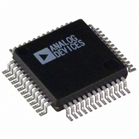
ADUC836BSZ Analog Devices Inc, ADUC836BSZ Datasheet - Page 28

ADUC836BSZ
Manufacturer Part Number
ADUC836BSZ
Description
16bit Dual ADC With Embedded 8 Bit MCU
Manufacturer
Analog Devices Inc
Series
MicroConverter® ADuC8xxr
Datasheet
1.ADUC836BSZ.pdf
(80 pages)
Specifications of ADUC836BSZ
Core Processor
8052
Core Size
8-Bit
Speed
12.58MHz
Connectivity
EBI/EMI, I²C, SPI, UART/USART
Peripherals
POR, PSM, PWM, Temp Sensor, WDT
Number Of I /o
34
Program Memory Size
62KB (62K x 8)
Program Memory Type
FLASH
Eeprom Size
4K x 8
Ram Size
2.25K x 8
Voltage - Supply (vcc/vdd)
2.7 V ~ 5.25 V
Data Converters
A/D 7x16b; D/A 1x12b
Oscillator Type
Internal
Operating Temperature
-40°C ~ 125°C
Package / Case
52-MQFP, 52-PQFP
Cpu Family
ADuC8xx
Device Core
8052
Device Core Size
8b
Frequency (max)
12.58MHz
Interface Type
I2C/SPI/UART
Total Internal Ram Size
2.25KB
# I/os (max)
26
Number Of Timers - General Purpose
3
Operating Supply Voltage (typ)
3.3/5V
Operating Supply Voltage (max)
5.25V
Operating Supply Voltage (min)
2.7V
On-chip Adc
2(2-chx16-bit)
On-chip Dac
1-chx12-bit
Instruction Set Architecture
CISC
Operating Temp Range
-40C to 125C
Operating Temperature Classification
Automotive
Mounting
Surface Mount
Pin Count
52
Package Type
MQFP
Package
52MQFP
Family Name
ADuC8xx
Maximum Speed
12.58 MHz
Operating Supply Voltage
3.3|5 V
Data Bus Width
8 Bit
Number Of Programmable I/os
26
Number Of Timers
3
Lead Free Status / RoHS Status
Lead free / RoHS Compliant
Lead Free Status / RoHS Status
Lead free / RoHS Compliant
Available stocks
Company
Part Number
Manufacturer
Quantity
Price
Company:
Part Number:
ADUC836BSZ
Manufacturer:
ADI
Quantity:
150
Company:
Part Number:
ADUC836BSZ
Manufacturer:
Analog Devices Inc
Quantity:
10 000
Part Number:
ADUC836BSZ
Manufacturer:
ADI/亚德诺
Quantity:
20 000
ADC Chopping
Both ADCs on the ADuC836 implement a chopping scheme
whereby the ADC repeatedly reverses its inputs. The decimated
digital output words from the Sinc
offset and negative offset term included.
As a result, a final summing stage is included in each ADC so that
each output word from the filter is summed and averaged with
the previous filter output to produce a new valid output result
to be written to the ADC data SFRs. In this way, while the ADC
throughput or update rate is as discussed earlier and illustrated in
Table VIII, the full settling time through the ADC (or the time to
a first conversion result) will actually be given by 2 t
The chopping scheme incorporated in the ADuC836 ADC results
in excellent dc offset and offset drift specifications and is extremely
beneficial in applications where drift, noise rejection, and optimum
EMI rejection are important factors.
Calibration
The ADuC836 provides four calibration modes that can be pro-
grammed via the mode bits in the ADCMODE SFR detailed in
Table V. In fact, every ADuC836 has already been factory cali-
brated. The resultant Offset and Gain calibration coefficients
for both the primary and auxiliary ADCs are stored on-chip in
manufacturing-specific Flash/EE memory locations. At power-on
or after reset, these factory calibration coefficients are automati-
cally downloaded to the calibration registers in the ADuC836
SFR space. Each ADC (primary and auxiliary) has dedicated
calibration SFRs, which have been described earlier as part of the
general ADC SFR description. However, the factory calibration
values in the ADC calibration SFRs will be overwritten if any
one of the four calibration options are initiated and that ADC is
enabled via the ADC enable bits in ADCMODE.
Even though an internal offset calibration mode is described
below, it should be recognized that both ADCs are chopped. This
chopping scheme inherently minimizes offset and means that an
internal offset calibration should never be required. Also, because
factory 5 V/25°C gain calibration coefficients are automatically
ADuC836
3
filters therefore have a positive
ADC
.
–28–
present at power-on an internal full-scale calibration will only be
required if the part is being operated at 3 V or at temperatures
significantly different from 25°C.
The ADuC836 offers internal or system calibration facilities. For
full calibration to occur on the selected ADC, the calibration
logic must record the modulator output for two different input
conditions: zero-scale and full-scale points. These points are
derived by performing a conversion on the different input volt-
ages provided to the input of the modulator during calibration.
The result of the zero-scale calibration conversion is stored in the
Offset Calibration Registers for the appropriate ADC. The result
of the full-scale calibration conversion is stored in the Gain Cali-
bration Registers for the appropriate ADC. With these readings,
the calibration logic can calculate the offset and the gain slope for
the input-to-output transfer function of the converter.
During an internal zero-scale or full-scale calibration, the respective
zero-scale input and full-scale inputs are automatically connected to
the ADC input pins internally to the device. A system calibration,
however, expects the system zero-scale and system full-scale volt-
ages to be applied to the external ADC pins before the calibration
mode is initiated. In this way, external ADC errors are taken into
account and minimized as a result of system calibration. It should
also be noted that to optimize calibration accuracy, all ADuC836
ADC calibrations are carried out automatically at the slowest
update rate.
Internally in the ADuC836, the coefficients are normalized before
being used to scale the words coming out of the digital filter. The
offset calibration coefficient is subtracted from the result prior to
the multiplication by the gain coefficient.
From an operational point of view, a calibration should be treated
like another ADC conversion. A zero-scale calibration (if required)
should always be carried out before a full-scale calibration. System
software should monitor the relevant ADC RDY0/1 bit in the
ADCSTAT SFR to determine end of calibration via a polling
sequence or interrupt driven routine.
REV. A


