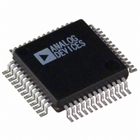
ADUC836BSZ Analog Devices Inc, ADUC836BSZ Datasheet - Page 18

ADUC836BSZ
Manufacturer Part Number
ADUC836BSZ
Description
16bit Dual ADC With Embedded 8 Bit MCU
Manufacturer
Analog Devices Inc
Series
MicroConverter® ADuC8xxr
Datasheet
1.ADUC836BSZ.pdf
(80 pages)
Specifications of ADUC836BSZ
Core Processor
8052
Core Size
8-Bit
Speed
12.58MHz
Connectivity
EBI/EMI, I²C, SPI, UART/USART
Peripherals
POR, PSM, PWM, Temp Sensor, WDT
Number Of I /o
34
Program Memory Size
62KB (62K x 8)
Program Memory Type
FLASH
Eeprom Size
4K x 8
Ram Size
2.25K x 8
Voltage - Supply (vcc/vdd)
2.7 V ~ 5.25 V
Data Converters
A/D 7x16b; D/A 1x12b
Oscillator Type
Internal
Operating Temperature
-40°C ~ 125°C
Package / Case
52-MQFP, 52-PQFP
Cpu Family
ADuC8xx
Device Core
8052
Device Core Size
8b
Frequency (max)
12.58MHz
Interface Type
I2C/SPI/UART
Total Internal Ram Size
2.25KB
# I/os (max)
26
Number Of Timers - General Purpose
3
Operating Supply Voltage (typ)
3.3/5V
Operating Supply Voltage (max)
5.25V
Operating Supply Voltage (min)
2.7V
On-chip Adc
2(2-chx16-bit)
On-chip Dac
1-chx12-bit
Instruction Set Architecture
CISC
Operating Temp Range
-40C to 125C
Operating Temperature Classification
Automotive
Mounting
Surface Mount
Pin Count
52
Package Type
MQFP
Package
52MQFP
Family Name
ADuC8xx
Maximum Speed
12.58 MHz
Operating Supply Voltage
3.3|5 V
Data Bus Width
8 Bit
Number Of Programmable I/os
26
Number Of Timers
3
Lead Free Status / RoHS Status
Lead free / RoHS Compliant
Lead Free Status / RoHS Status
Lead free / RoHS Compliant
Available stocks
Company
Part Number
Manufacturer
Quantity
Price
Company:
Part Number:
ADUC836BSZ
Manufacturer:
ADI
Quantity:
150
Company:
Part Number:
ADUC836BSZ
Manufacturer:
Analog Devices Inc
Quantity:
10 000
Part Number:
ADUC836BSZ
Manufacturer:
ADI/亚德诺
Quantity:
20 000
ADCMODE (ADC Mode Register)
Used to control the operational mode of both ADCs.
SFR Address
Power-On Default Value
Bit Addressable
Bit
7
6
5
4
3
2
1
0
NOTES
1. Any change to the MD bits will immediately reset both ADCs. A write to the MD2–0 bits with no change is also treated as a reset. (See exception to this in Note 3.)
2. If ADC0CON is written when ADC0EN = 1, or if ADC0EN is changed from 0 to 1, then both ADCs are also immediately reset. In other words, the primary ADC is
3. On the other hand, if ADC1CON is written or if ADC1EN is changed from 0 to 1, only the auxiliary ADC is reset. For example, if the primary ADC is continuously converting
4. Once ADCMODE has been written with a calibration mode, the RDY0/1 bits (ADCSTAT) are immediately reset and the calibration commences. On completion, the appropriate
5. Any calibration request of the auxiliary ADC while the temperature sensor is selected will fail to complete. Although the RDY1 bit will be set at the end of the calibration
6. Calibrations are performed at maximum SF (see SF SFR) value, guaranteeing optimum calibration operation.
ADuC836
given priority over the auxiliary ADC, and any change requested on the primary ADC is immediately responded to.
when the auxiliary ADC change or enable occurs, the primary ADC continues undisturbed. Rather than allow the auxiliary ADC to operate with a phase difference from
the primary ADC, the auxiliary ADC will fall into step with the outputs of the primary ADC. The result is that the first conversion time for the auxiliary ADC will be
delayed up to three outputs while the auxiliary ADC update rate is synchronized to the primary ADC.
calibration registers are written, the relevant bits in ADCSTAT are written, and the MD2–0 bits are reset to 000 to indicate the ADC is back in Power-Down mode.
cycle, no update of the calibration SFRs will take place and the ERR1 bit will be set.
Name
–––
–––
ADC0EN
ADC1EN
–––
MD2
MD1
MD0
Description
Reserved for Future Use
Reserved for Future Use
Primary ADC Enable.
Set by the user to enable the primary ADC and place it in the mode selected in MD2–MD0, below.
Cleared by the user to place the primary ADC in power-down mode.
Auxiliary ADC Enable.
Set by the user to enable the auxiliary ADC and place it in the mode selected in MD2–MD0, below.
Cleared by the user to place the auxiliary ADC in power-down mode.
Reserved for Future Use
Primary and Auxiliary ADC Mode bits.
These bits select the operational mode of the enabled ADC as follows:
MD2
0
0
0
0
1
1
1
1
MD1
0
0
1
1
0
0
1
1
D1H
00H
No
MD0
0
1
0
1
0
1
0
1
Table V. ADCMODE SFR Bit Designations
ADC input(s).
ADC0/1CON Register.
ADC0/1CON Register.
ADC Power-Down Mode (Power-On Default)
Idle Mode. The ADC filter and modulator are held in a reset state although the
modulator clocks are still provided.
Single Conversion Mode. A single conversion is performed on the enabled ADC.
On completion of the conversion, the ADC data registers (ADC0H/M and/or ADC1H/L)
are updated, the relevant flags in the ADCSTAT SFR are written, and power-down is
re-entered with the MD2–MD0 accordingly being written to 000.
Continuous Conversion. The ADC data registers are regularly updated at the selected
update rate (see SF Register).
Internal Zero-Scale Calibration. Internal short automatically connected to the enabled
Internal Full-Scale Calibration. Internal or external V
and XREF1 bits in ADC0/1CON) is automatically connected to the enabled ADC
input(s) for this calibration.
System Zero-Scale Calibration. User should connect system zero-scale input to the
enabled ADC input(s) as selected by CH1/CH0 and ACH1/ACH0 bits in the
System Full-Scale Calibration. User should connect system full-scale input to the
enabled ADC input(s) as selected by the CH1/CH0 and ACH1/ACH0 bits in the
–18–
REF
(as determined by XREF0
REV. A


