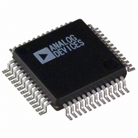
ADUC836BSZ Analog Devices Inc, ADUC836BSZ Datasheet - Page 46

ADUC836BSZ
Manufacturer Part Number
ADUC836BSZ
Description
16bit Dual ADC With Embedded 8 Bit MCU
Manufacturer
Analog Devices Inc
Series
MicroConverter® ADuC8xxr
Datasheet
1.ADUC836BSZ.pdf
(80 pages)
Specifications of ADUC836BSZ
Core Processor
8052
Core Size
8-Bit
Speed
12.58MHz
Connectivity
EBI/EMI, I²C, SPI, UART/USART
Peripherals
POR, PSM, PWM, Temp Sensor, WDT
Number Of I /o
34
Program Memory Size
62KB (62K x 8)
Program Memory Type
FLASH
Eeprom Size
4K x 8
Ram Size
2.25K x 8
Voltage - Supply (vcc/vdd)
2.7 V ~ 5.25 V
Data Converters
A/D 7x16b; D/A 1x12b
Oscillator Type
Internal
Operating Temperature
-40°C ~ 125°C
Package / Case
52-MQFP, 52-PQFP
Cpu Family
ADuC8xx
Device Core
8052
Device Core Size
8b
Frequency (max)
12.58MHz
Interface Type
I2C/SPI/UART
Total Internal Ram Size
2.25KB
# I/os (max)
26
Number Of Timers - General Purpose
3
Operating Supply Voltage (typ)
3.3/5V
Operating Supply Voltage (max)
5.25V
Operating Supply Voltage (min)
2.7V
On-chip Adc
2(2-chx16-bit)
On-chip Dac
1-chx12-bit
Instruction Set Architecture
CISC
Operating Temp Range
-40C to 125C
Operating Temperature Classification
Automotive
Mounting
Surface Mount
Pin Count
52
Package Type
MQFP
Package
52MQFP
Family Name
ADuC8xx
Maximum Speed
12.58 MHz
Operating Supply Voltage
3.3|5 V
Data Bus Width
8 Bit
Number Of Programmable I/os
26
Number Of Timers
3
Lead Free Status / RoHS Status
Lead free / RoHS Compliant
Lead Free Status / RoHS Status
Lead free / RoHS Compliant
Available stocks
Company
Part Number
Manufacturer
Quantity
Price
Company:
Part Number:
ADUC836BSZ
Manufacturer:
ADI
Quantity:
150
Company:
Part Number:
ADUC836BSZ
Manufacturer:
Analog Devices Inc
Quantity:
10 000
Part Number:
ADUC836BSZ
Manufacturer:
ADI/亚德诺
Quantity:
20 000
I
The ADuC836 supports a fully licensed* I
I
ware master. SDATA (Pin 27) is the data I/O pin and SCLOCK
(Pin 26) is the serial clock. These two pins are shared with the
MOSI and SCLOCK pins of the on-chip SPI interface.Therefore
I2CCON
SFR Address
Power-On Default Value
Bit Addressable
Bit
7
6
5
4
3
2
1
0
I2CADD
Function
SFR Address
Power-On Default Value
Bit Addressable
I2CDAT
Function
SFR Address
Power-On Default Value
Bit Addressable
*Purchase of licensed I
ADuC836
2
Patent Rights to use these components in an I
2
C SERIAL INTERFACE
C interface is implemented as a full hardware slave and soft-
Name
MDO
MDE
MCO
MDI
I2CM
I2CRS
I2CTX
I2CI
2
C components of Analog Devices or one of its sublicensed associated companies conveys a license for the purchaser under the Philips I
Description
I
This data bit is used to implement a master I
be output on the SDATA pin if the data output enable (MDE) bit is set.
I
Set by user to enable the SDATA pin as an output (Tx).
Cleared by user to enable SDATA pin as an input (Rx).
I
This data bit is used to implement a master I
be output on the SCLOCK pin.
I
This data bit is used to implement a master I
latched into this bit on SCLOCK if the data output enable (MDE) bit is 0.
I
Set by user to enable I
Cleared by user to enable I
I
Set by user to reset the I
Cleared by user code for normal I
I
Set by MicroConverter if the interface is transmitting.
Cleared by the MicroConverter if the interface is receiving.
I
Set by the MicroConverter after a byte has been transmitted or received.
Cleared automatically when the user code reads the I2CDAT SFR (see I2CDAT below).
2
2
2
2
2
2
2
2
C Software Master Data Output Bit (Master Mode Only).
C Software Master Data Output Enable Bit (Master Mode Only).
C Software Master Clock Output Bit (Master Mode Only).
C Software Master Data Input Bit (Master Mode Only).
C Master/Slave Mode Bit.
C Reset Bit (Slave Mode Only).
C Direction Transfer Bit (Slave Mode Only).
C Interrupt Bit (Slave Mode Only).
I
Holds the I
at
9BH
55H
No
I
The I2CDAT SFR is written by the user to transmit data over the I
data just received by the I
and the I2CI bit in the I2CCON SFR. User software should access I2CDAT only once per interrupt cycle.
9AH
00H
No
2
2
C Address Register
C Data Register
www.analog.com/microconverter
2
I
E8H
00H
Yes
C system provided that the system conforms to the I
2
2
C peripheral address for the part. It may be overwritten by the user code. Application Note uC001
C Control Register
2
C serial interface. The
Table XXII. I2CCON SFR Bit Designations
2
C software Master mode.
2
C interface.
2
2
C hardware Slave mode.
C interface. Accessing I2CDAT automatically clears any pending I
2
C operation.
describes the format of the I
–46–
2
2
2
the user can enable only one interface or the other at any given
time (see SPE in Table XXI). Application Note uC001 describes
the operation of this interface as implemented and is available from
the MicroConverter website at: www.analog.com/microconverter.
Three SFRs are used to control the I
described below.
C transmitter interface in software. Data written to this bit will
C transmitter interface in software. Data written to this bit will
C receiver interface in software. Data on the SDATA pin is
2
C Standard Specification as defined by Philips.
2
C standard 7-bit address in detail.
2
C interface or read by user code to read
2
C interface. These are
2
C interrupt
2
C
REV. A


