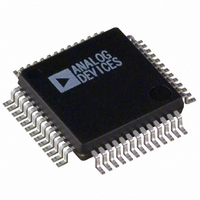
ADUC836BSZ Analog Devices Inc, ADUC836BSZ Datasheet - Page 71

ADUC836BSZ
Manufacturer Part Number
ADUC836BSZ
Description
16bit Dual ADC With Embedded 8 Bit MCU
Manufacturer
Analog Devices Inc
Series
MicroConverter® ADuC8xxr
Datasheet
1.ADUC836BSZ.pdf
(80 pages)
Specifications of ADUC836BSZ
Core Processor
8052
Core Size
8-Bit
Speed
12.58MHz
Connectivity
EBI/EMI, I²C, SPI, UART/USART
Peripherals
POR, PSM, PWM, Temp Sensor, WDT
Number Of I /o
34
Program Memory Size
62KB (62K x 8)
Program Memory Type
FLASH
Eeprom Size
4K x 8
Ram Size
2.25K x 8
Voltage - Supply (vcc/vdd)
2.7 V ~ 5.25 V
Data Converters
A/D 7x16b; D/A 1x12b
Oscillator Type
Internal
Operating Temperature
-40°C ~ 125°C
Package / Case
52-MQFP, 52-PQFP
Cpu Family
ADuC8xx
Device Core
8052
Device Core Size
8b
Frequency (max)
12.58MHz
Interface Type
I2C/SPI/UART
Total Internal Ram Size
2.25KB
# I/os (max)
26
Number Of Timers - General Purpose
3
Operating Supply Voltage (typ)
3.3/5V
Operating Supply Voltage (max)
5.25V
Operating Supply Voltage (min)
2.7V
On-chip Adc
2(2-chx16-bit)
On-chip Dac
1-chx12-bit
Instruction Set Architecture
CISC
Operating Temp Range
-40C to 125C
Operating Temperature Classification
Automotive
Mounting
Surface Mount
Pin Count
52
Package Type
MQFP
Package
52MQFP
Family Name
ADuC8xx
Maximum Speed
12.58 MHz
Operating Supply Voltage
3.3|5 V
Data Bus Width
8 Bit
Number Of Programmable I/os
26
Number Of Timers
3
Lead Free Status / RoHS Status
Lead free / RoHS Compliant
Lead Free Status / RoHS Status
Lead free / RoHS Compliant
Available stocks
Company
Part Number
Manufacturer
Quantity
Price
Company:
Part Number:
ADUC836BSZ
Manufacturer:
ADI
Quantity:
150
Company:
Part Number:
ADUC836BSZ
Manufacturer:
Analog Devices Inc
Quantity:
10 000
Part Number:
ADUC836BSZ
Manufacturer:
ADI/亚德诺
Quantity:
20 000
Parameter
EXTERNAL PROGRAM MEMORY
REV. A
t
t
t
t
t
t
t
t
t
t
t
t
LHLL
AVLL
LLAX
LLIV
LLPL
PLPH
PLIV
PXIX
PXIZ
AVIV
PLAZ
PHAX
ALE Pulsewidth
Address Valid to ALE Low
Address Hold after ALE Low
ALE Low to Valid Instruction In
ALE Low to PSEN Low
PSEN Pulsewidth
PSEN Low to Valid Instruction In
Input Instruction Hold after PSEN
Input Instruction Float after PSEN
Address to Valid Instruction In
PSEN Low to Address Float
Address Hold after PSEN High
PORT 0 (I/O)
CORE_CLK
PORT 2 (O)
PSEN (O)
ALE (O)
Figure 71. External Program Memory Read Cycle
t
LHLL
t
AVLL
(OUT)
PCL
t
t
LLAX
LLPL
12.58 MHz Core_Clk
Min
119
39
49
49
193
0
0
t
AVIV
–71–
t
PLAZ
PCH
Max
218
133
54
292
25
t
PLPH
t
t
LLIV
PLIV
INSTRUCTION
(IN)
t
PXIX
Min
2t
t
t
t
3t
0
0
CORE
CORE
CORE
CORE
CORE
t
PXIZ
– 40
– 30
– 30
Variable Core_Clk
– 40
– 45
t
PHAX
Max
4t
3t
t
5t
25
CORE
CORE
CORE
CORE
– 25
– 100
– 105
– 105
ADuC836
Unit
ns
ns
ns
ns
ns
ns
ns
ns
ns
ns
ns
ns


